


News: Microelectronics
9 April 2020
Boosting output power in aluminium gallium nitride channel transistors
Ohio State University and University of South Carolina in the USA claim the highest radio frequency (RF) output power density ever reported for aluminium-rich aluminium gallium nitride (AlGaN)-channel transistors [Hao Xue et al, IEEE Electron Device Letters, published 3 March 2020]. The power density was 2.7W/mm at 10GHz.
AlGaN is a natural progression from the GaN transistors being developed for high-voltage/high-power/high-frequency switching and amplification deployment. As the Al-content of the AlGaN alloy increases, the bandgap increases, along with the correlated critical electrical breakdown field.
The researchers used a ‘micro-channel’ heterostructure field-effect transistor (HFET) architecture to enhance electron injection by the source contact. The researchers comment: “Here we show the challenges of high contact resistance can be mitigated to a significant extent by increasing the relative periphery of contacts through the use of multi-constriction channels.”
The researchers used metal-organic chemical vapor deposition (MOCVD) to prepare an epitaxial sample on sapphire (Figure 1). The 50nm Al0.65Ga0.35N barrier was doped with silicon (Si) at a nominal concentration of 2x10¹⁸/cm3.
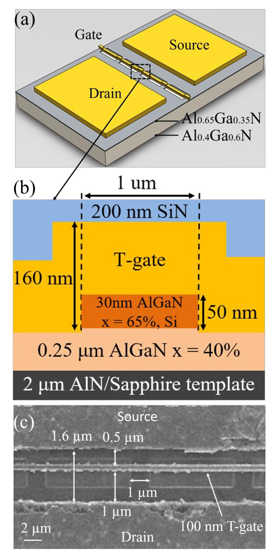
Figure 1: (a) Device scheme. (b) Cross-sectional view. (c) Top-view scanning electron micrograph before SiN passivation showing device geometry of 1:6 (active/non-active region) and device dimensions.
Fabrication began with ohmic contact formation: surface oxide removal using hydrochloric acid solution, electron-beam evaporation deposition of zirconium/aluminium/molybdenum/gold, and 900°C annealing for 45 seconds in nitrogen.
Next, the team performed plasma etch to create the mesa device isolation. A hard mask to protect the micro-channel regions, consisting of 50nm silicon dioxide, was deposited using plasma-enhanced CVD (PECVD). Further plasma etch removed the AlGaN barrier layer except for the micro-channel. After etch, the hard mask was removed with a buffered oxide etch.
The T-gate of the device consisted of nickel/gold patterned and formed using electron-beam lithography and lift-off processing. Device passivation was supplied by a 200nm layer of silicon nitride (SiN) deposited using PECVD.
The gate-source, gate-drain and source-drain spacings were 0.5μm, 1μm and 1.6μm, respectively. The gate length (Lg) was 100nm. The width of the individual micro-channels was 1μm. The effective channel width of the complete device was 15.6μm. The device width, including non-active regions, was 100μm.
A 900mA/mm maximum drain current density, normalized to the effective width, was achieved at 10V drain bias and 2V gate potential. Comparison planar HFETs achieved 480mA/mm, normalized to the total width. The on-resistance was 6.35Ω-mm for the micro-channel devices, while the conventional HFETs registered 11.9Ω-mm with the gate at 2V.
The 140mS/mm peak transconductance of the micro-channel transistors was an 80% improvement over the conventional devices. The team credits superior source electron injection for the enhanced performance.
The breakdown voltages with a 10mA/mm threshold were 80V and 33V for the micro-channel and conventional HFETs, respectively. The gate was set at -15V. The drain current varied over a wider range in the conventional HFET, starting from around 10-3mA/mm and progressing up to 10mA/mm. By contrast, the micro-channel device varied just an order of magnitude before reaching the breakdown threshold.
The researchers comment: “Clearly, the breakdown of planar devices is dominated by the drain-induced barrier lowering (DIBL) effect with an onset bias of ~3.5V that is suppressed in micro-channel devices. Therefore, we attribute this to the improvement of short-channel effect in micro-channel HFETs.”
The micro-channel HFET suffered from a high gate leakage over that range to breakdown, attributed to surface states at the plasma-etch fin sidewalls.
Small-signal RF measurements gave cut-off (fT) and maximum oscillation (fmax) values of 20GHz and 36GHz, respectively, for the micro-channel HFET. The corresponding values for the conventional HFET were 25GHz and 30GHz. The bias point was -2V on the gate and 13V on the drain. The team suspects that parasitic capacitance is responsible for the lower fT of the micro-channel device. The low fTxLg product for both devices is blamed on the high sheet resistance of AlGaN and the large source-drain distance of 1.6μm. Scaling would improve the RF performance, it is suggested.
Large-signal continuous-wave load-pull measurements gave a power density of 2.7W/mm for the micro-channel HFET at -1.5V gate and 30V drain bias. The conventional device achieved 0.85W/mm at -1.5V gate and 15V drain bias.
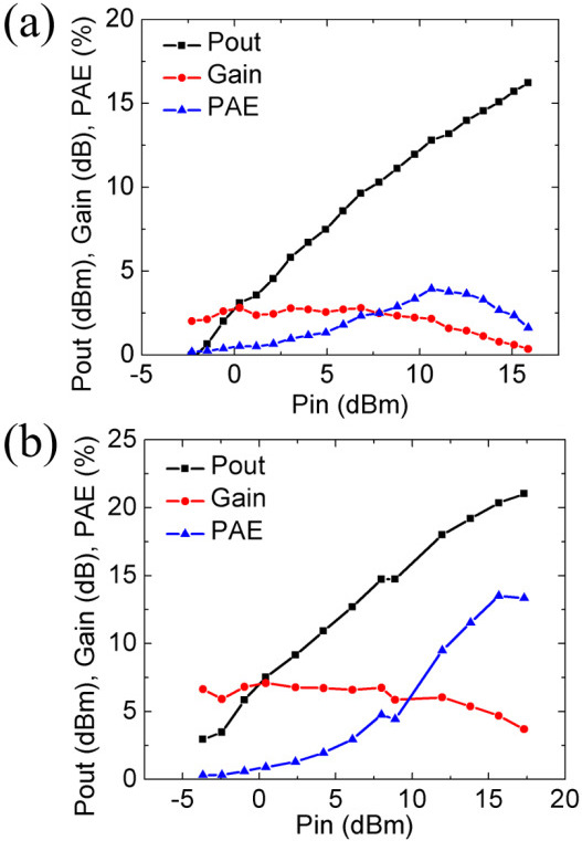
Figure 2: RF output power (Pout), associated gain, and PAE at 10GHz of (a) micro-channel and (b) planar HFETs.
The team reports: “The RF output power of Al0.65Ga0.35N/Al0.4Ga0.6N micro-channel HFETs reported here is the highest value ever reported of Al-rich AlGaN channel transistors.”
The micro-channel power-added efficiency (PAE), however, was only 4%. This is attributed to low power gain and gain compression effects. The researchers point to a trade-off between current density and device peripheral dimensions.
The team writes: “For practical applications, depending on the target current and power level, the chip size may be larger. However, these questions can be better answered down the road as the device technology becomes more mature.”
AlGaN channel transistors HFET MOCVD AlGaN PECVD
https://doi.org/10.1109/LED.2020.2977997
The author Mike Cooke is a freelance technology journalist who has worked in the semiconductor and advanced technology sectors since 1997.


