


News: Microelectronics
28 April 2020
Eta demos GaN-on-GaN epitaxy of vertical power device structures
Vertical gallium nitride (GaN) power devices hold the potential to revolutionize the power device industry, notes Eta Research of Shanghai, China, which was founded in 2015 to develop free-standing GaN wafers. There is particular interest for higher-voltage applications (such as 600V and above) for vertical GaN devices. According to the physical properties of the materials, GaN devices have a lower specific on-resistance for a given breakdown voltage compared with traditional silicon power devices and newer native silicon carbide (SiC) power devices. As proof of the material benefits, horizontal GaN power devices – namely GaN-on-Si HEMTs – have seen success in competing with silicon in the low-voltage market.
It is expected that vertical GaN power devices will compete with native SiC power devices for the high-voltage market. In the last two years, SiC devices have been gaining market share for high-voltage applications and several companies have expanded the production of 6” and 8” SiC wafers. In contrast, vertical GaN power devices are not yet sold commercially, and GaN wafers are available in 4” diameter from only a handful of suppliers. The expanded supply and reliable quality of GaN wafers will be important for the development of vertical GaN power devices.
There are three potential advantages of GaN compared with SiC for high-voltage power devices. Firstly, for a given breakdown voltage, the theoretical specific on-resistance is about an order of magnitude less. Therefore, the power losses during forward bias could be reduced and the efficiency would be higher. Secondly, for a given breakdown voltage and on-resistance, the device size will be smaller. The smaller size means that many more devices can be made on a wafer, reducing the cost. Additionally, a smaller form factor is more desirable for most applications. Lastly, GaN holds an advantage in the maximum frequency at which a power device can operate, which is determined by both the materials properties and device design. Generally, for SiC the maximum frequency may be about 1MHz or less. GaN power devices will be able to operate at much higher frequencies, at least tens of MHz, which is a frequency range that is inaccessible to SiC. Higher-frequency operation is beneficial to reduce the size of passive components, and thereby reduce the size, weight and cost of the power conversion system.
Vertical GaN power devices are still in the R&D phase of development. There is no consensus within the GaN research community regarding the optimal device structure for GaN vertical power devices. The three leading potential device structures include the current-aperture vertical electron transistor, trench FET, and fin FET. All of the device structures include a lightly doped N-layer as the drift layer. This layer is important because the thickness of the drift layer determines the breakdown voltage of the device and the electron concentration has an important role in achieving the theoretical lowest specific on-resistance.
Eta manufactures and sells 4” free-standing GaN wafers, which are available in both n-type conductivity and semi-insulating form. The company also offers metal-organic chemical vapor deposition (MOCVD) epitaxy of GaN structures on GaN wafers. Customers developing vertical GaN power devices have similar requirements for their device structures, especially concerning the thickness and doping of the drift layer. First, the drift layer should have a thickness of about 10μm or more, which is required to ensure that the breakdown voltage is sufficient to meet the device design criteria. Next, the surface of the drift layer should be smooth enough to create planar interfaces for the subsequent device layers. Last, the drift layer must have a low electron concentration, typically in the range of 1E16–5E16/cm3.
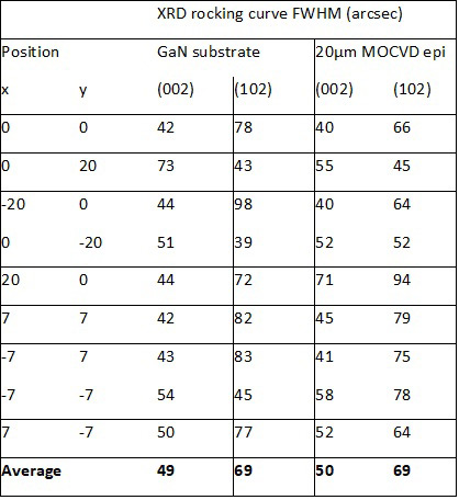
Figure 1: X-ray diffraction data.
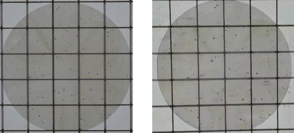
Figure 2: 2” GaN wafer before and after 20μm GaN epitaxy.
The company has performed experiments for GaN-on-GaN epitaxy in the range of 10–20μm thickness. Figures 1 and 2 show the x-ray diffraction (XRD) data and wafer pictures for 20μm of GaN grown by MOCVD on a 2” GaN wafer. A 9-point pattern was used for XRD measurement of the rocking curve FWHMs of the 002 and 102 peaks. The average values of the rocking curve FWHMs before epitaxy were 49 arcsec and 69 arcsec for the 002 and 102 peaks, respectively. After the 20μm epitaxy, the rocking curve FWHMs were nearly identical, with average values of 50 arcsec and 69 arcsec for the same two peaks. The bow of the wafer was slightly improved after epitaxy, starting at –5.0μm before epitaxy and resulting in –1.3μm after epitaxy.
A relatively smooth surface can be achieved by appropriate selection of the offcut. An offcut of 0.4° toward the m-plane was selected. For 10μm film growth on the 0.4°-offcut GaN wafer, the average surface roughness was 8–16nm, measured by Bruker optical interferometry over an area of 239μm x 318μm. Figure 3 shows an optical Nomarski image of a featureless surface and Figure 4 shows the optical interferometry image.
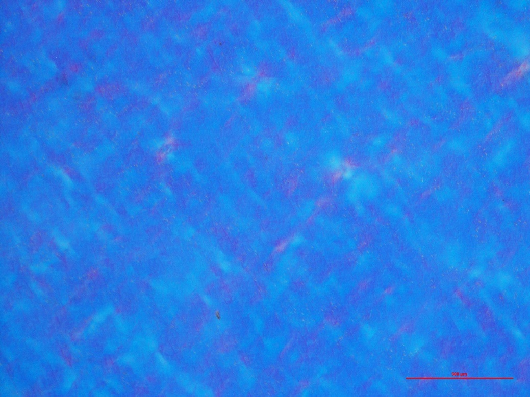
Figure 3: Nomarski optical microscope image, showing a relatively featureless surface.
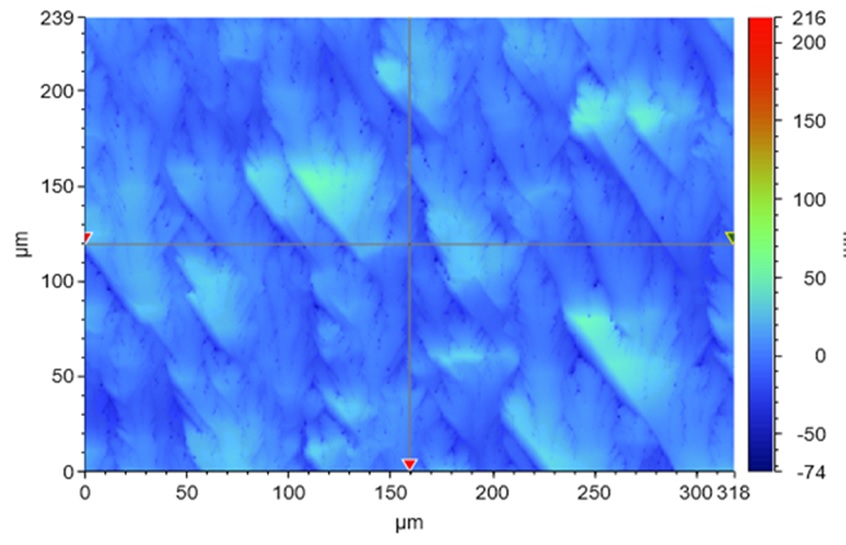
Figure 4: Bruker optical interferometer image of the epitaxy surface.
The low electron concentration of the drift layer may not be readily achievable under the typical MOCVD growth conditions used for LEDs. The drift layer must also have a growth rate that is sufficiently high to obtain a thick MOCVD layer within a reasonable time frame. The company has undertaken studies to achieve a low-electron-concentration drift layer. The lowest electron concentration achieved has been 2E15/cm3, measured using the capacitance–voltage (C–V) method. Additional silicon dopant can be added to the MOCVD growth to achieve higher electron concentrations.
Eta is now able to offer GaN-on-GaN MOCVD epitaxy layers suitable for vertical GaN power devices. The GaN homoepitaxy drift layers can be grown over 10μm thick with a relatively smooth surface and electron concentration in the 1015–1016/cm3 range. Device structures can also be grown with multiple layers including InGaN, AlGaN, n-type doping, and p-type doping. Other potential device structures include LEDs and lasers diodes grown on n-type GaN wafers and HEMTs grown on semi-insulating GaN wafers.
Eta develops 4” semi-insulating GaN wafers
Eta launches polished epi-ready 100mm n-type GaN wafers


