

News: Microelectronics
5 October 2026
Navitas and Microchip collaborate on 800V reference design for AI data centers
As AI data centers scale to support high-power GPU clusters, the industry is shifting toward 800V DC rack power architectures to improve distribution efficiency, increase power density and support next-generation server designs. To help accelerate this transition, power semiconductor firm Navitas Semiconductor Corp of Torrance, CA, USA and Microchip Technology Inc of Chandler, AZ, USA have collaborated on an 800V DC-to-6V DC reference design for AI data-center rack power applications.
The platform combines Microchip’s digital power control and security technologies with Navitas’ GaNFast gallium nitride (GaN) power devices to give developers a practical path to implement high-efficiency power conversion aligned with the Open Compute Project (OCP) 800V DC standard. Complete with reference hardware, software and design documentation, the solution helps to reduce design risk, shorten development cycles and accelerate deployment of next-generation AI infrastructure.
“AI infrastructure optimization is driving one of the most significant power architecture transitions the data-center industry has experienced in decades,” notes Joe Thomsen, corporate VP of Microchip’s digital signal controller business unit. “As the ecosystem moves toward higher-voltage rack power systems, developers need proven building blocks that help reduce design risk and accelerate innovation. Our collaboration with Navitas brings together complementary technologies to help customers navigate this transition and bring next-generation power solutions to market more quickly.”
At the core of the reference platform are Microchip’s dsPIC33AK digital signal controllers (DSCs), TA100 CryptoAuthentication device, and Navitas’ GaNFast FETs. The dsPIC33AK is designed to provide high-resolution control, high-speed analog and security with support for post-quantum cryptography. The devices offer library support for Commercial National Security Algorithm (CNSA) Suite 2.0 recommended post-quantum cryptographic (PQC) algorithms and feature hardware accelerated cryptographic functions needed in Open Compute Project (OCP) power supplies and other connected real‑time control designs. Powered by a 200MHz 32-bit core with a double-precision floating-point unit (FPU), the dsPIC33AK256MPS306 family combines 78ps high-resolution pulse width modulators (PWMs) and multiple 12-bit analog-to-digital converters (ADCs) operating at up to 40MSPS. The high-speed core and peripherals support fast, deterministic control loops for high-frequency, high-efficiency DC/DC power conversion.
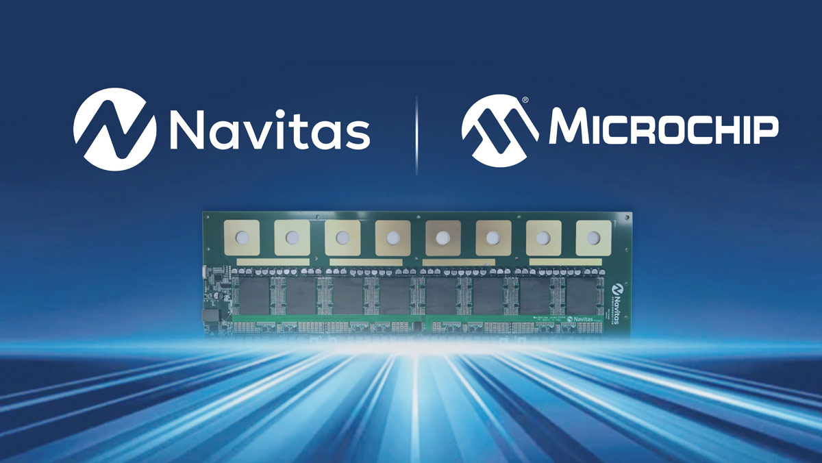
This PDB is powered by 16 x NV6034, 650V, 17mΩ GaNFast FETs in a stacked half-bridge topology on the primary side. The DFN8x8 dual-side-cooled package extends the performance advantages of GaN by reducing thermal resistance, allowing higher continuous power operation while maintaining exceptional efficiency. The PDB targets delivering up to 96% peak efficiency at full load with 1MHz switching frequency, enabling a power density of 2100W/in3.
About 20% thinner than a mobile phone, its ultra-low profile enables extremely close integration with the GPU board, maximizing transient performance and improving power distribution efficiency. Navitas says that its system-level approach ensures that advances in GaN technology translate into measurable improvements in efficiency, power density, transient performance, and total cost of ownership. Direct conversion from 800V DC to 6V DC combines both 800V DC-to-50V DC and 50V DC-to-6V DC conversion stages into one converter, delivering higher end-to-end efficiency.
“As AI infrastructure scales to support increasingly demanding computing platforms, Navitas’ GaNFast technology is a critical enabler of higher power density, greater efficiency, and improved system performance,” says Vipin Bothra, VP of global solution marketing at Navitas. “By combining Navitas’ leadership in power semiconductors with Microchip’s digital control expertise, this collaboration accelerates the delivery of advanced power solutions tailored to the evolving requirements of next-generation AI data centers.”
The reference design also incorporates Microchip’s TA100 CryptoAuthentication device to help address growing security requirements within modern power infrastructure. By integrating hardware-based security into the design, developers can establish a trusted foundation for system authentication and protection without the complexity of implementing security measures from scratch. The TA100 device provides support for code authentication (secure boot), Message Authentication Code (MAC) generation, trusted firmware updates, multiple key management protocols including Transport Layer Security (TLS) and other root-of-trust-based operations.
The Microchip and Navitas reference design provides a platform for developing high-voltage, high-power, compact rack power systems for AI data centers. The design combines power control, security and GaN power technologies to support efficient 800V-to-6V-power conversion while helping system developers to address evolving power delivery, performance and form-factor requirements. The solution is being showcased at Microchip’s event at the 2026 Open Compute Project (OCP) Global Summit in San Jose, CA, USA (12–15 October).
The design will be supported with a reference board, software and supporting documentation, giving developers access to the resources needed to evaluate and accelerate deployment of 800V DC power conversion systems for AI data-center applications.
Navitas debuts 800V–6V DC–DC power delivery board at NVIDIA GTC