


News: Microelectronics
20 August 2025
D-band GaN power HEMTs on silicon
Researchers based in Singapore have reported the first gallium nitride (GaN) high-electron-mobility transistors on silicon (Si) substrates designed to operate in the D-band (110-170GHz) radio frequency (RF) range at the sub-THz level above 0.1 terahertz (100GHz) [Hanchao Li et al, IEEE Electron Device Letters, published online 21 July 2025]. They comment: “This demonstration marks the highest frequency (and the first-time reaching D-band) in power amplification among published GaN-on-Si HEMTs.”
The team — variously associated with Singapore’s Nanyang Technological University, the National Semiconductor Translation and Innovation Centre for Gallium Nitride (NSTIC (GaN)), Institute of Microelectronics (IME), National University of Singapore, and Singapore-MIT Alliance for Research and Technology — comments: “This work pushes the boundaries of GaN-on-Si HEMT technology by demonstrating its feasibility for D-band power amplification, for the first time.”
Potential advantages of using silicon substrates include large wafer diameter availability, cost-effectiveness, and compact integration with silicon CMOS. Such devices are strong candidates for low-cost sub-THz 6G cellular infrastructure. Other sub-THz applications include atmospheric remote sensing, and THz power sources based on frequency multiplier chains.
The material for the HEMT (Figure 1) was grown by metal-organic chemical vapor deposition (MOCVD) on high-resistivity (HR) silicon substrate, and included a 4nm in-situ SiN layer. A double-heterostructure channel of 4nm/150nm/100nm AlN/GaN/Al0.08Ga0.92N was designed to suppress short-channel effect, enabling high-frequency performance.
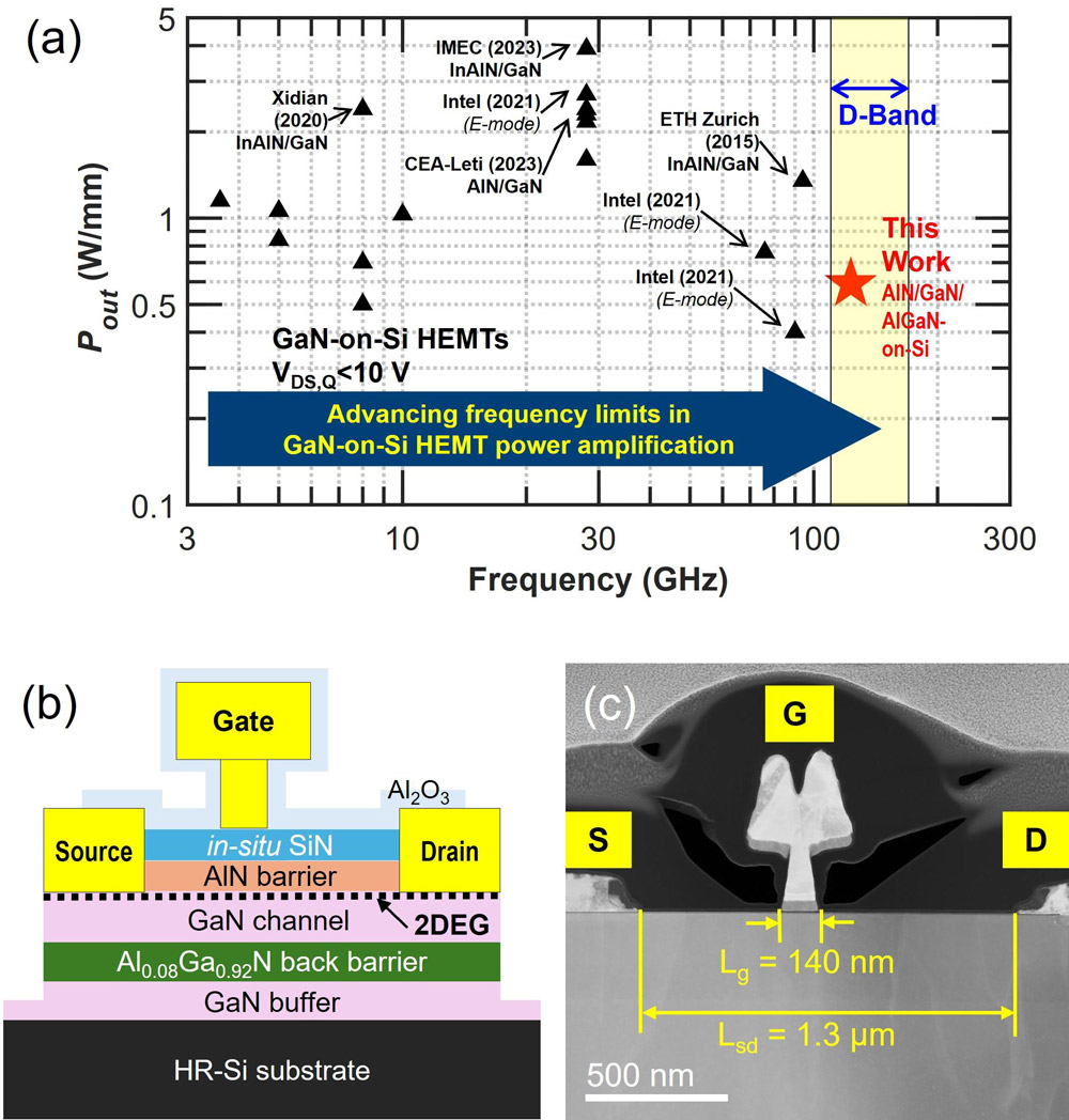
Figure 1: (a) Benchmark of output power (Pout) at drain bias (Vds) up to 10V against frequency of GaN-on-Si HEMTs. (b) AlN/GaN/AlGaN-on-Si MIS-HEMT scheme. (c) Cross-sectional transmission electron microscopy (TEM) image of fabricated device.
The use of AlN as top barrier, rather than AlGaN, increased the carrier density in the two-dimensional electron gas (2DEG) channel that forms near the AlN/GaN interface, due to a larger conduction-band offset and stronger polarization effects. Hall-effect measurements reported 1.7x10¹³/cm2 sheet charge density, and 1400cm2/V-s mobility. The sheet resistance was 260Ω/□.
The fabrication process included mesa isolation by inductively coupled plasma reactive-ion etching, annealed titanium/aluminium/nickel/gold deposition for the ohmic source/drain contacts, nickel/gold T-gate formation, and atomic layer deposition of aluminium oxide (Al2O3) passivation.
The in-situ SiN layer was preserved throughout the fabrication process, serving in the final HEMT as a gate dielectric, and minimizing interface contamination (e.g. protecting the Al in the top barrier from oxidation) and defect formation. The researchers also point out that the thin (14nm) SiN/Al2O3 stack minimized parasitic capacitances.
The gate length (Lg) was 140nm. The placement of the gate was 480nm from the source (Lg), and 680nm from the drain (Lgd). The total source–drain distance (Lsd) was thus 1.3μm. The gate width consisted of two fingers of 16μm (2x16μm).
The team comments: “The small finger width was intended to minimize signal propagation delay (’transverse delay’) while maintaining low gate resistance, which is critical for minimizing RF signal attenuation along the gate finger and improving the maximum oscillation frequency (fmax).”
DC characterization resulted in 2.0A/mm maximum drain current density, 1.1Ω-mm on-resistance, −2V threshold voltage, 105 on/off current ratio, and 0.65S/mm peak transconductance.
The three-terminal breakdown occurred at 35V, attributed to ionization of carriers at the drain edge of the gate, leading to a sudden increase in both drain and gate currents.
Current collapse was assessed in pulsed measurements with −5V gate pulses superimposed on the quiescent state (Vgq), and simultaneous gate/drain pulses of −5V/5V, respectively. The gate pulsing resulted in 8.6% collapse, and the combined pulsing in 15.2%.
Small-signal RF characterization showed a cut-off frequency (fT) of 112GHz, while fmax came in at 205GHz.
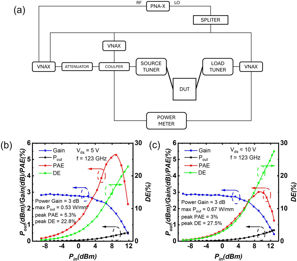
Figure 2: RF large-signal performance at 123GHz continuous wave (CW). (a) Measurement setup with tuning at fundamental frequency. (b) Power sweep results at 5V Vds. (c) Power sweep results at 10V Vds.
The RF large-signal performance was tested using an on-wafer D-band passive load-pull system (Figure 2). The peak power-added efficiency (PAE) of 5.3% was achieved at 0.36W/mm output power with 5V drain bias. The maximum output power was 0.67W/mm at 10V drain bias.
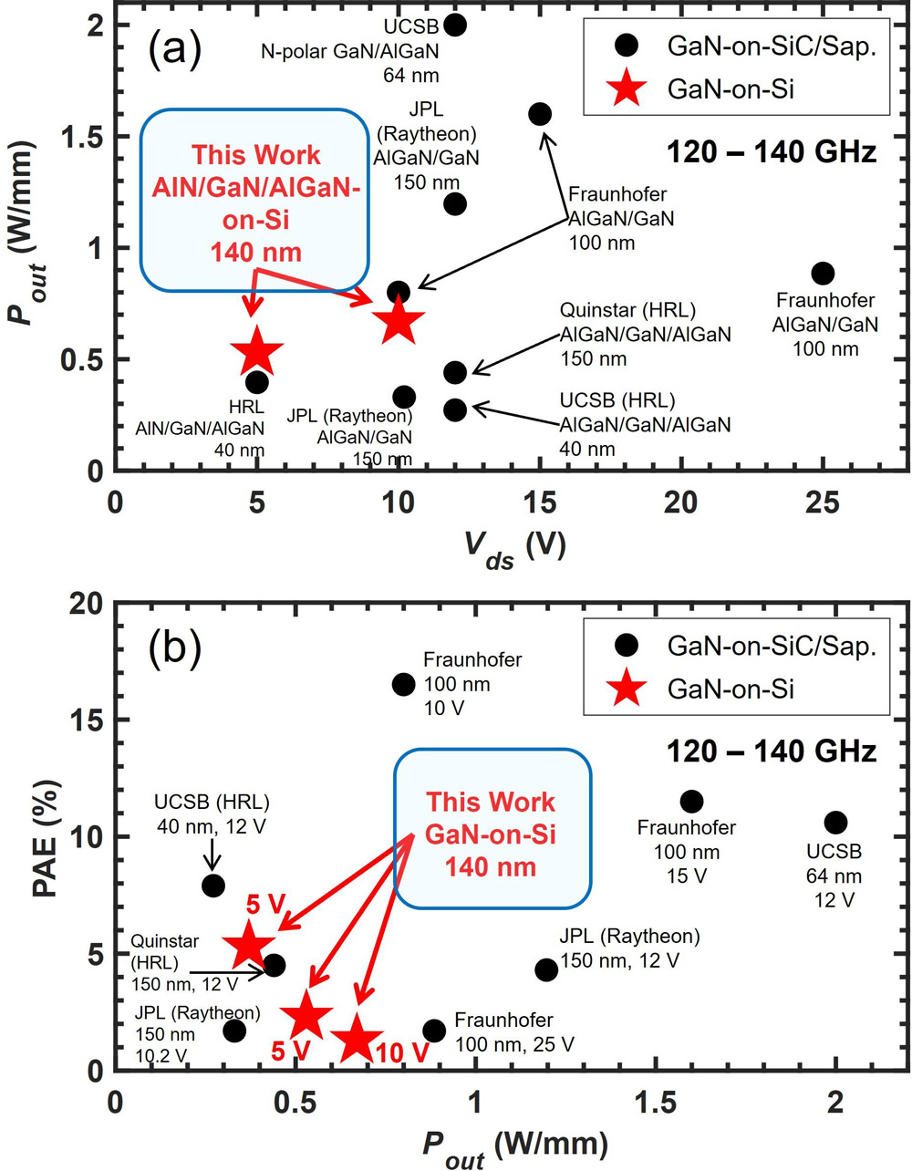
Figure 3: RF large-signal benchmarks against GaN on SiC or sapphire: (a) Pout versus Vds; (b) PAE versus Pout. Foundries, if used, appear in parentheses.
The team also compare their work with HEMTs in pre-matched monolithic microwave ICs (MMICs) on silicon carbide (SiC) or sapphire (Figure 3). The researchers admit that this is not completely fair since these devices are often the result of trade-offs designed to achieve certain other aims at the expense of efficiency or output power, adding that their purpose is “to provide technological context rather than a direct performance benchmark”. Even so, the plots show competitive performance relative to devices on the more expensive alternative substrates.
The team suggests the relatively low PAE was mainly due to “parasitic losses induced by melt-back etching into the silicon substrate during epitaxial growth”. Improvements could be delivered by regrown contacts, optimized passivation, the use of active tuning, or multi-finger gates. According to the team, multi-finger gates would be needed to scale up output power while maintaining efficiency.
Singapore opens NSTIC (GaN), first national facility for gallium nitride
https://doi.org/10.1109/LED.2025.3591141
www.a-star.edu.sg/ime/Research/power-electronics
The author Mike Cooke is a freelance technology journalist who has worked in the semiconductor and advanced technology sectors since 1997.


