


News: Microelectronics
9 July 2025
Singapore opens NSTIC (GaN), first national facility for gallium nitride
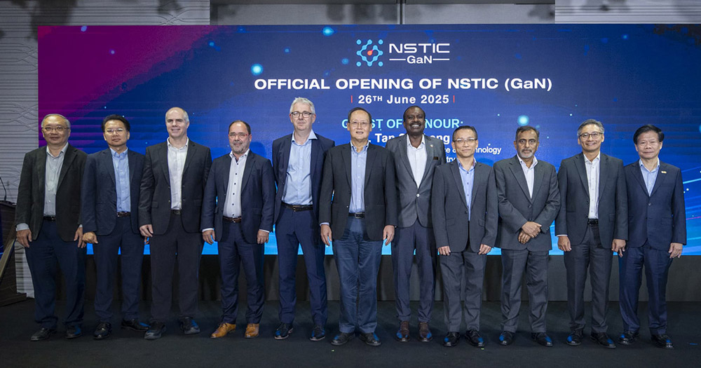
Singapore’s Minister-in-charge of Energy and Science & Technology Dr Tan See Leng has officially opened the National Semiconductor Translation and Innovation Centre for Gallium Nitride (NSTIC (GaN)) as Singapore’s first national facility dedicated to gallium nitride.
First set up in 2023 as the National Gallium Nitride Technology Centre (NGTC), NSTIC (GaN) is a partnership between Singapore’s Agency for Science, Technology and Research (A*STAR), DSO National Laboratories, and Nanyang Technological University, Singapore (NTU Singapore).
The center brings advanced GaN manufacturing capabilities to Singapore, aiming to position local innovators to compete in high-growth global markets such as advanced 5G and 6G communication systems, radars and satellite communications.
The center addresses common challenges faced by companies and researchers – such as limited local access to advanced facilities and the need for closer collaboration across the ecosystem – by providing industry and research collaborators with access to advanced wafer fabrication and prototyping infrastructure.
Boosting Singapore’s semiconductor innovation ecosystem
NSTIC (GaN) is part of the broader National Semiconductor Translation and Innovation Centre (NSTIC) initiative led by A*STAR, which supports national efforts to deepen semiconductor R&D and innovation across priority domains such as photonics and advanced packaging.
NSTIC (GaN) was established to build national capabilities in this critical technology area, and to support companies in translating GaN innovation into real-world impact. The center will offer access to infrastructure and R&D capabilities to help startups, SMEs and MNCs to prototype, validate and scale up competitive and commercially relevant GaN-based technologies.
First national facility for both 6-inch GaN-on-SiC and 8-inch GaN-on-silicon
NSTIC (GaN) is the first facility in Singapore to host both 6-inch GaN-on-silicon carbide and 8-inch GaN-on-silicon wafer fabrication lines. This dual capability allows it to serve a wide range of applications with varying performance requirements.
It will also offer advanced GaN technology with gate length below 0.1μm and operation frequencies above 100GHz, which allows for very fast processing speeds. It is reckoned that this will place Singapore among a select group of global locations with the infrastructure to produce advanced semiconductors that will power future communication and advanced instrumentation technology.
From mid-2026, NSTIC (GaN) will begin offering commercial foundry services for prototyping and fabrication. This will enable companies to carry out advanced development work locally, reducing reliance on overseas facilities and accelerating their time-to-market, it is expected. The availability of such infrastructure in Singapore should help to lower capital and technology barriers — especially for start-ups and SMEs — and support the growth of a more self-sufficient semiconductor innovation ecosystem.
“NSTIC (GaN) is not just a facility — it is a national platform for innovation and a catalyst for future technologies,” says Cheong Chee Hoo, chairman of the NSTIC (GaN) steering committee. “Our goal is to build deep capabilities in GaN manufacturing and research.”
Strengthening industry collaboration and local supply chains
Industry partnerships are a key part of NSTIC (GaN)’s approach, enabling it to co-develop technologies, strengthen local capabilities, and support strategic access to critical materials.
One such collaboration involves WaferLead, a local start-up working with NSTIC (GaN) to develop high-quality silicon carbide substrates — a key component in GaN wafer production. This partnership will support the development and enhancement of wafer performance, quality and reliability, while strengthening local capabilities and Singapore’s supply chain resilience.
As part of the launch, several memoranda of understanding (MoUs) and research collaboration agreements (RCAs) will be signed between NSTIC (GaN) and industry partners. These collaborations span areas such as substrate development, high-frequency circuit design, advanced packaging, and fabrication process enhancement.
Developing a pipeline of local semiconductor talent
NSTIC (GaN) plays a strategic role in developing a pipeline of local semiconductor talent. Through partnerships with Singapore’s Institutes of Higher Learning (IHLs), it offers students and researchers early exposure to industry-grade infrastructure and processes, equipping them with practical experiences in the semiconductor sector.
The center also supports PhD training programs in collaboration with IHLs and industry, helping to deepen translational research capabilities in GaN technologies. These efforts are critical to ensuring that Singapore has the talent base needed to support the growth of its deep-tech innovation ecosystem, it is reckoned.


