


News: Optoelectronics
19 January 2023
Integrating nanowire lasers in hybrid polymer-SiN waveguides
Northwestern Polytechnical University in China and Australian National University report on progress in integrating on-chip nanowire (NW) laser sources in passive photonic integrated circuits (PICs) [Ruixuan Yi et al, Nano Letters, v22, p9920, 2022].
The researchers implemented a straightforward strategy to embed the NWs in a waveguide (Figure 1). First, indium phosphide (InP) nanowires were transferred to a 3μm-thick silicon dioxide (SiO2) substrate with a thin 300nm silicon nitride (SiN) top layer. Gold markers were incorporated into the substrate to aid nanowire placement with a tungsten probe. The quantum-confined nanowires themselves can be produced in processes with high quality. The team used nanowires from metal-organic vapor-phase epitaxy on a (111)A InP substrate.
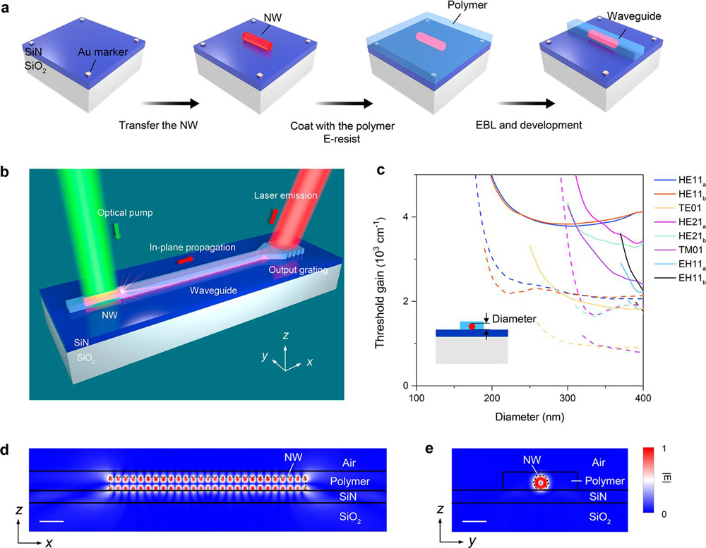
Figure 1: (a) Integration process flow for nanowire laser embedded in hybrid polymer-SiN waveguide. (b) InP nanowire laser integrated with hybrid polymer-SiN waveguide. (c) Threshold gain in air (dashed lines) of different guided modes and embedded in hybrid waveguide (solid lines) versus nanowire diameter with inset cross-section. (d) and (e) xz and yz plane cross-sections, respectively, of electric field distribution of TE01 resonant mode supported by nanowire laser (4.47μm length, 310nm diameter). Scale bars: 500nm.
The researchers comment: “This integration strategy of an on-chip laser is applicable to other PIC platforms, such as silicon and lithium niobate, and the top cladding layer could be changed by depositing SiN or SiO2, promising its CMOS compatibility.” They add: “Nanowire lasers have the merits of an ultracompact footprint, low threshold, and low energy consumption.”
Although the nanowires were manipulated into position, the team believes that “large-scale integration of multiple nanowire lasers could be achieved once the positions of nanowires were determined, which does not require the manipulation of individual nanowires one by one. In future device development, a nanowire array could be grown directly with controllable positions on the slab or arranged properly through an automated transfer printing technique, promising the large-scale integration of the waveguide-embedded nanowire lasers.”
After placement, the nanowires were covered with 400nm polymer electron-beam lithography (EBL) resist by spin coating. EBL and development embedded the nanowire in a hybrid polymer-SiN photonic structure, supporting in-plane light propagation. The team suggests that there are standard alignment techniques, which could precisely locate the wires in the waveguide during the EBL.
The nanowires had a high refractive index around 3.45, allowing the use of the end facets as the mirrors of a Fabry-Perot laser cavity.
In a basic PIC setup with an optically pumped nanowire laser at one end and an output grating at the other of a 180μmx1.7μm waveguide, the laser threshold pump fluence was 37.3μJ/cm2 from a 532nm pulsed laser at 10K. The spectral peak of the laser emission was at 827nm wavelength. By consulting polarization measurements and simulations, the researchers attribute the laser emission to the transverse electric TE01 mode. The team also used similar techniques to determine the coupling efficiency from the nanowire laser TE01 mode to the TE-bound mode of the hybrid waveguide at 2.3%. The researchers subjected the structure to a 3 hour run and found no observable degradation in performance.
The researchers fabricated a range of other PIC structures. In one, the nanowire laser fed in to a Y-splitter that demonstrated roughly 50-50 power splitting. The laser threshold in this case was 21.7μJ/cm2. The team sees the ability to split power in this way leading to “more complicated structures, such as modulators based on a Mach-Zehnder interferometer, optical phase arrays, etc.”
With a view to wave-division multiplexing, the researchers also fabricated a multiplexer with three nanowire laser feeds (Figure 2). The lasers showed peak wavelengths at 828.8nm, 828.4nm and 835.8nm.
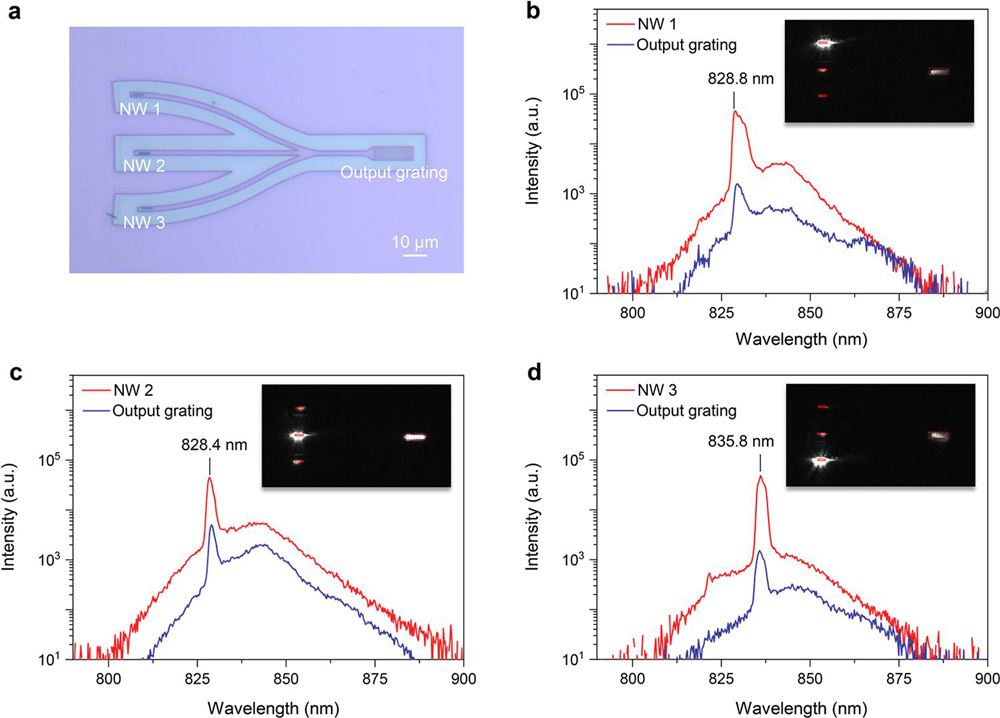
Figure 2: (a) Optical microscope image of wavelength multiplexer integrated with three nanowires. (b-d). Spectra collected from nanowires and output grating under excitations on NW 1 (b), NW 2 (c), and NW 3 (d) above lasing threshold, respectively, with inset panchromatic images.
The coupling efficiencies of the demonstrated PICs were limited to less than 5%, due to the mismatch between the nanowire lasing mode and the hybrid waveguide mode. “Most of the light from the nanowire laser radiates to the free space rather than couples to the waveguide mode,” the team explains. Simulations suggest that, by varying the dimensions of the nanowire and waveguide, coupling efficiencies up to 28% could be reached, coupling the helical HE11a mode of a 150nm-diameter nanowire to the transverse magnetic mode of the waveguide.
At present, the devices only operate stably at the very low temperature of 10K, probably due to “overheating induced by the polymer cladding”. The researchers comment: “By properly designing a heat sink in the waveguide-embedded nanowire, it is expected to increase the lasing operation temperature to 300K: for example, the nanowire could be embedded in a silicon nitride waveguide, which has a much higher thermal conductive coefficient than the polymer.”
On-chip nanowire laser sources Photonic integrated circuits SiN InP EBL
The author Mike Cooke is a freelance technology journalist who has worked in the semiconductor and advanced technology sectors since 1997.


