


News: Optoelectronics
10 November 2022
Very-near-infrared InP QD laser diodes on silicon
Hong Kong University of Science and Technology (HKUST) has demonstrated electrically pumped quantum dot (QD) lasers grown on (001) silicon with pulsed lasing around 750nm wavelength, very near infrared, at room temperature and up to 95°C [Wei Luo et al, Optics Express, v30, p40750, 2022].
The dots consisted of indium phosphide (InP) in a gallium arsenide phosphide (GaAsP) quantum well (QW) with aluminium gallium arsenide (AlGaAs) barriers. The team sees potential for display, bio-photonics, and spatial mapping applications.
The researchers comment: “Embedding InP QDs in the simple ternary GaAsP/AlGaAs QW systems provides an efficient and reliable light source with emission wavelength at ~750nm on silicon, paving the way toward the integration with silicon photonics for a variety of applications near the infrared.”
The team adds: “InP QD lasers on silicon with emission wavelength at 650–750nm are seldom explored.”
HKUST also hopes that the achievements of visible red-emitting QD lasers on GaAs substrates may soon be transferred to (001) Si without offcut measures, often used to improve growth quality, as needed for integration with mainstream silicon complementary metal-oxide-semiconductor (CMOS) electronics and photonics.
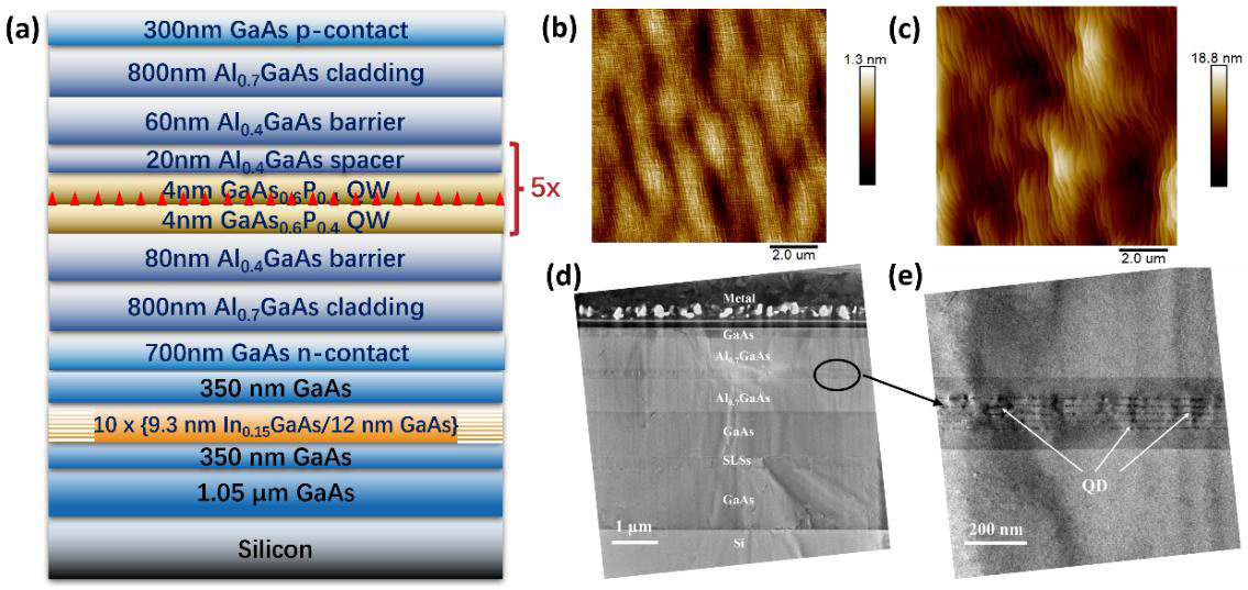
Figure 1: (a) Electrically pumped InP/GaAsP QD laser scheme on GaAs/Si template. Atomic force micrographs (AFMs) InP/GaAsP QDs grown on (b) GaAs and (c) GaAs/Si templates with 0.18nm and 2.76nm surface roughness, respectively. (d) Cross-sectional transmission electron micrographs (TEMs) of electrically pumped InP/GaAsP QD laser grown on GaAs/Si template. (e) Zoom-in cross-sectional TEM.
The QD laser structures (Figure 1) were grown on GaAs/Si templates by metal-organic chemical vapor deposition (MOCVD). The templates were prepared by a separate MOCVD process where a number of steps were taken to reduce defects arising from lattice mismatch such as thermal cycle annealing and InGaAs/GaAs strain-layer superlattice insertions. The template layer was 2μm thick with a threading dislocation density (TDD) of 2.8x107cm2 and a 1.3nm surface roughness. The 2μm thickness is seen as a trade-off between TDD and the risk of crack generation.
The researchers found that five-layer QD in well structures grown at 680°C resulted in stronger photoluminescence than ones with three layers or those grown at 690°C. The lower growth temperature was particularly critical, giving around 4x emission intensity. The center wavelength was around 736nm.
Reference samples were also grown on GaAs substrates in the same process chamber at the same time.
The material was fabricated into ridge-waveguide edge-emitting laser diodes. The devices were subjected to 400ns pulsed operation with a 0.5% duty cycle. The devices had a 1.4V turn-on voltage. The laser threshold current density was as low as 573A/cm2 on reference 70μmx2mm laser diodes on GaAs substrate (Figure 2). The threshold was somewhat higher on the GaAs/Si templates at 657A/cm2. The laser wavelength at 20°C was 757nm.
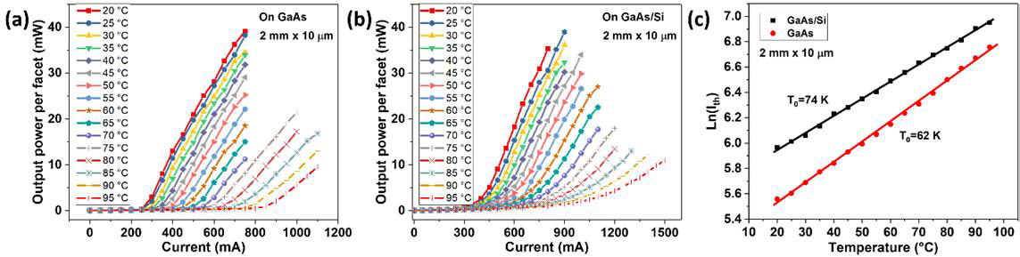
Figure 2: (a) Temperature-dependent light output power-current curves of 2mmx10μm InP/GaAsP QD lasers grown on (a) GaAs and (b) GaAs/Si templates, respectively. (c) Characteristic temperature graph.
Lasing continued in both types of device up to the 95°C temperature limit of the experimental setup. The characteristic temperatures of the devices were 62K and 74K for laser diodes on GaAs and GaAs/Si, respectively. A higher characteristic temperature, as seen in the GaAs/Si laser diodes, indicates a slower increase of the lasing threshold with increased temperature (a good thing).
The HKUST team comments: “The characteristic temperature of the InP/GaAsP QD laser grown on the GaAs/Si template is higher than that on GaAs, which may be a result of better thermal dissipation of silicon.”
Quantum dot lasers InP GaAsP quantum well AlGaAs barriers GaAs substrate MOCVD
The author Mike Cooke is a freelance technology journalist who has worked in the semiconductor and advanced technology sectors since 1997.


