


News: Microelectronics
9 December 2022
Toshiba develops SiC MOSFET with check-pattern embedded Schottky barrier diodes
At the 68th annual IEEE International Electron Devices Meeting (IEDM 2022) in San Francisco (3–7 December), Japan-based Toshiba Electronic Devices & Storage Corp (TDSC) – spun off from Toshiba Corp in 2017 – reported the development of a silicon carbide (SiC) metal–oxide–semiconductor field-effect transistor (MOSFET) that arranges embedded Schottky barrier diodes (SBD) in a check pattern (check-pattern embedded SBD) to realize both low on-resistance and high reliability. Toshiba has confirmed that the design secures an approximately 20% reduction in on-resistance (RonA) against its existing SiC MOSFET, with no loss of reliability.
Silicon carbide is widely seen as the next-generation material for power devices, as it delivers higher voltages and lower losses than silicon. While use of SiC is now largely limited to inverters for trains, wider application is on the horizon, in areas including vehicle electrification and the miniaturization of industrial equipment. However, a problem that must first be overcome is that bipolar conduction in the body diode during reverse operation of SiC MOSFETs is harmful because it degrades on-resistance.
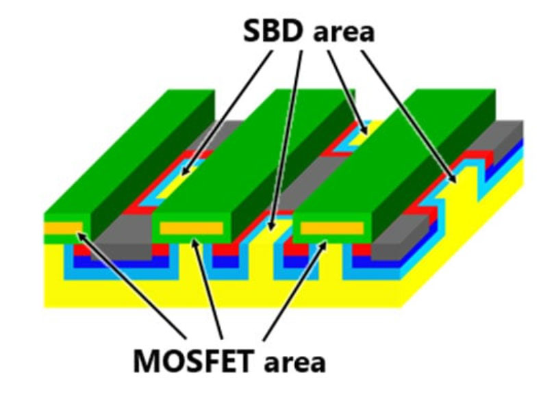
Picture: Schematic diagram of MOSFETs with newly developed check pattern embedded SBD-SiC MOSFET.
Toshiba Electronic Devices & Storage Corp developed a device structure that embeds SBDs into the MOSFET to inactivate body diodes, but it found that replacing the MOSFET channel with an embedded SBD lowers channel density and increases RonA. This trade-off has now been resolved with a new embedded SBD structure, and Toshiba has confirmed that it dramatically improves performance characteristics.
Toshiba has improved both conduction loss in its SBD-embedded SiC MOSFET and achieved good diode conductivity, by deploying a check-pattern SBD distribution. Evaluation of the on-side current characteristics of 1.2kV-class-SBD-embedded MOSFETs with the optimized design confirmed that using the check design to position the embedded-SBDs close to the body diodes effectively limits bipolar conduction of the parasitic diodes, while the unipolar current limit of reverse conduction is double that realized by the existing striped SBD pattern design for the same SBD area consumption. RonA was found to be about 20% lower, at 2.7mΩ.cm2.
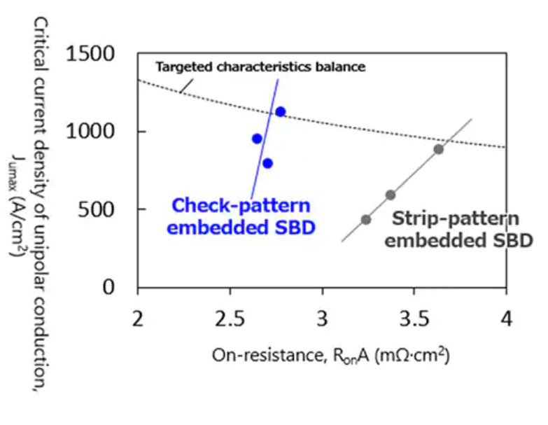
Picture: Trade-off of characteristics of 1.2kV-class SiC MOSFET.
This confirmed improvement in the trade-off is essential if SiC MOSFETs are to be used in inverters for motor-drive applications. Toshiba is continuing to carry out evaluations toward improving dynamic characteristics and reliability, and to develop attractive, high-performance power semiconductors that contribute to carbon neutrality.
Toshiba launches third-generation SiC MOSFETs


