


- News
29 December 2015
Pushing vertical p-n junctions toward gallium nitride critical field
University of Notre Dame and Cornell University have reported more details on their work towards high-performance gallium nitride (GaN) vertical structures [Meng Qi et al, Appl. Phys. Lett., vol107, p232101, 2015]: "GaN vertical p-n junctions with off-state leakage current as low as 3nA/cm2, breakdown field Ebr~3.1 MV/cm, and Ron~0.23mΩ-cm2 are achieved in epitaxial diodes. These breakdown and leakage characteristics represent the highest performance metrics in GaN p-n junction diodes grown by MBE."
The researchers used bulk GaN substrates to reduce threading dislocation densities (TDDs). Such defects cause premature breakdown of electron devices. The estimated peak electric field in some of their devices of 3.1MV/cm was derived on the basis of simulations. They comment: "This electric field of 3.1MV/cm is close to the estimated critical field of 3.5–3.8MV/cm for GaN. It is among the highest experimental results reported."
The devices were grown using molecular beam epitaxy (MBE), which has a number of advantages over metal-organic chemical vapor deposition (MOCVD). The researchers see potential benefits from MBE's high degree of control of alloy compositions, high-quality aluminium nitride (AlN) layers and heterostructures, and efficient magnesium (Mg) acceptor doping for buried p-type layers that do not need activation annealing.
A disadvantage of MBE tends to be its slower growth rate compared with MOCVD or hydride vapor phase epitaxy (HVPE). Higher growth rates can be achieved with plasma rather than ammonia MBE, allowing thicker drift layers to be achieved. Thicker layers should lead to higher breakdown voltages by reducing the peak electric field.
The researchers also observed strong electroluminescence (EL) from their devices, indicating the high quality of the material. They add: "Since we can design for light to carry away a significant fraction of energy out of the diode, it can prove to be a very attractive way for device cooling in power electronics: a technique that has not been possible in indirect-bandgap power semiconductors such as Si and SiC diodes and transistors before."
Si and SiC are semiconductors with an indirect bandgap where recombination in pn diodes produces heat rather than photons. In Schottky diodes with metal-semiconductor junctions, carrier transport is through thermionic emission of electrons from the semiconductor into the metal. Heat generation in Schottky devices occurs in the metal where electrons dump their energy.
The researchers hope their work will lead to superior three-terminal GaN power switches using vertical p-n junctions, reaching towards the theoretical limits of GaN's critical field. Present lateral devices that operate in a unipolar manner (that is, not based on p-n junctions) tend to breakdown through gate leakage and allied effects, and not because of the intrinsic avalanche mechanism that gives the high critical field based on GaN's wide bandgap.
The pn structures (Figure 1) were grown on GaN substrates with three different levels of threading dislocation density: 1-2x10⁷/cm3, 2-5x10⁵/cm3, and 5x10⁴/cm3. The MBE growth was carried out on the metal-polar (Ga) face of the substrate. An extensive surface preparation cleaning and outgasing procedure was carried out over several hours to remove contaminants. The MBE began with a pure Ga flux soak to give a Ga-rich surface.
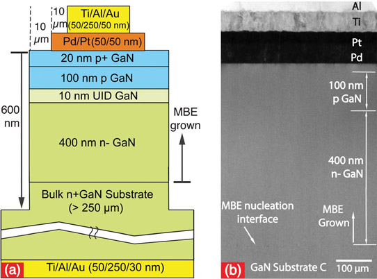
Figure 1: (a) Schematic structure and (b) cross-section TEM of fabricated vertical MBE-grown p-n diodes on low-dislocation-density bulk GaN crystal substrate C (TDD~5x10⁴/cm3).
The 400nm GaN buffer layer was grown using plasma-assisted MBE at 720°C. The nitrogen plasma was created using a 200W RF power source. The Mg and Al cells of the MBE equipment were kept heated at suitable standby temperatures to avoid oxygen outgasing into the reaction chamber.
Oxygen acts as a donor dopant in GaN. Breakdown voltages in vertical GaN devices are very sensitive to doping density, and the researchers wanted careful control of the unintentional doping (UID) level. In particular, they wanted a high acceptor over donor ratio so that the bulk of the depletion/drift region was on the n-side. The team achieved an acceptor/donor density ratio around 100.
The 10nm UID GaN layer was grown with the temperature ramping down from 720°C to 600°C. At the same time, the Mg cell temperature was increased from 200°C to 400°C to prepare for the growth of the p-GaN layers.
Excess Ga drops on the surface of the epitaxial material was removed using hydrochloric acid. Diode mesas were formed with reactive ion etching to a depth of 600nm. The n-electrode metals were applied to the back-side of the wafer. After deposition of the p-electrode metals, the devices were annealed at 400°C for 10 minutes. The fabrication was completed with the deposition of titanium/aluminium/gold (Ti/Al/Au) metal pads on the p-electrodes.
Electroluminescence for substrate B (TDD 2-5x10⁵/cm3) was found with wavelength peaks around 3.2eV and 2.2eV with 330A/cm2 injection, +5V bias. The 3.2eV radiation was associated with 3.4eV electron-hole recombination in the depletion region and photon absorption and re-emission from electrons droping to the Mg acceptor levels ~0.2eV above the valence band in the p-GaN. The 2.2eV radiation was attributed to deep-level transitions.
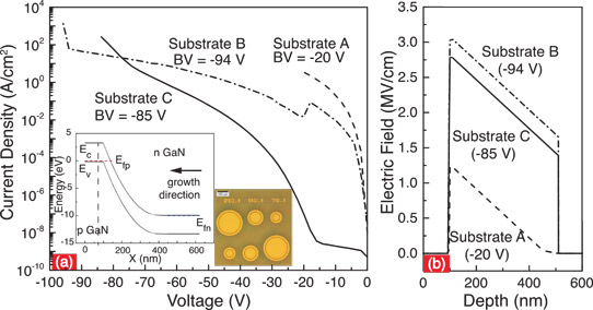
Figure 2: (a) Semilog plot of I-V characteristics with reverse bias voltages until breakdown for three vertical GaN p-n junctions on different GaN substrates. Inset figures show energy band diagram with 10V bias, as well as the image of fabricated diodes under optical microscope. (b) Electric field profiles along vertical direction of three p-n junctions on different substrates at corresponding breakdown voltages.
Diodes on substrate C with the lowest TDD level of less than 104/cm3 showed extremely low current densities of less 1nA/cm2 in the +2V to -5V region (Figure 2). The on/off current ratio for +5V/-5V bias was 1013. Diodes on the higher TDD substrates A and B had reverse current leakage of around 10-4A/cm2 density and on/off ratio around 108. The highest breakdown voltage of 94V was for substrate B diodes. The low-TDD substrate C diode had a slight reduced breakdown at 85V reverse bias.
Details of the mechanism for reverse bias breakdown are still under investigation.
Notre Dame and Cornell, with IQE, have very recently reported on other GaN vertical p-n diode characteristics such as ideality, recombination lifetime, and breakdown [www.semiconductor-today.com/news_items/2015/dec/cornell_241215.shtml; www.semiconductor-today.com/news_items/2015/dec/iqe-notredame-cornell_231215.shtml].
http://dx.doi.org/10.1063/1.4936891
The author Mike Cooke is a freelance technology journalist who has worked in the semiconductor and advanced technology sectors since 1997.


