


- News
24 December 2015
Bulk gallium nitride vertical diode powers over rival semiconductors
The universities of Cornell and Notre Dame in the USA have developed p-n diodes on bulk gallium nitride (GaN) with a claimed record 'figure-of-merit' (FOM) combination of breakdown voltage and on-resistance (Ron) [Zongyang Hu et al, Appl. Phys. Lett., vol107, p243501, 2015]. Also, the current-voltage profiles and temperature-dependent modelling suggest a long Shockley-Read-Hall (SRH) lifetime.
Lateral GaN devices on sapphire, silicon carbide or silicon have been developed for power switching and conversion. However, vertical structures could avoid such problems as field and current crowding that lead to breakdown. Bulk single-crystal GaN enables such vertical devices, and much progress in this direction has been made in the past few months.
The researchers comment: "The long SRH lifetime and low Ron in GaN demonstrated in this work indicate possibilities to design GaN p-n diodes utilizing the bipolar benefits of the material. Performance far beyond the unipolar limit predicted by FOM might be achievable in GaN bipolar power devices."
The epitaxial structures were prepared using metal-organic chemical vapor deposition (MOCVD) on bulk GaN substrate with defect density of ~106/cm2. The upper p-type layers were 400nm of magnesium-doped GaN:Mg and a heavily-doped (p++) cap. Hall-effect measurements determined the hole concentration in the p-type layers at 7x10¹⁶/cm3. The hole mobility was 24cm2/V-s.
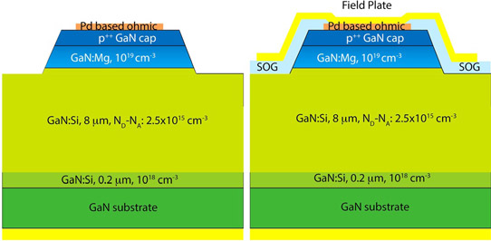
Figure 1: Schematic cross-sections of GaN p-n junction diodes: (left) without passivation/field plates and (right) with field plates.
The diode fabrication (Figure 1) included a circular bevel mesa structure for edge termination to avoid surface leakage currents. Devices were also produced with spin-on-glass passivation and field plates to further improve edge-termination performance and increase reverse-bias breakdown voltages. Devices without passivation or field plates were used in capacitance-voltage analysis of the junction built-in voltage and net carrier concentrations.
The forward current density for a 107μm-diameter bottom of the bevel mesa at 6V was 'close' to 9.3kA/cm2, based on a 117μm effective diameter to allow for current spreading (Figure 2). The differential on-resistance was around 0.12mΩ-cm2.
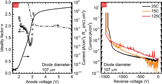
Figure 2: (a) Forward current-voltage characteristics at RT measured on GaN p-n diodes with mesa diameter of 107μm. (b) Temperature-dependent reverse current-voltage characteristics and breakdown voltages.
The researchers comment: "The on/off current ratio is about 14 orders of magnitude (limited by our measurement setup), thanks to minimized defects in GaN." The ideality factor made a transition from around 2.0 at 2.0V to 1.1 at 2.8V. Ideality around 2 suggests domination of non-radiative Shockley-Read-Hall recombination through charge traps. Ideality factors around 1 are associated with diffusion currents and radiative electron-hole recombination. However, reported radiative recombination coefficients suggest that this effect would have been negligible in the voltage range studied. The SRH lifetime was estimated at around 12ns at room temperature. The recombination center concentration was calculated to be 3x10¹⁵/cm3.
"Near-unity ideality factors in GaN observed over a temperature window have never been reported previously," the researchers add. "The near unity ideality factor is enabled by two primary facts: (1) a small SRH recombination current inside the depletion region due to a long SRH recombination lifetime, i.e. low concentrations of recombination centers; (2) low parasitic resistances allow diffusion current (η = 1) to dominate over a wide bias window."
The reverse-bias breakdown occurred at 1406V at room temperature (300K). This increased to 1442V at 350K and 1470V at 400K.
"The positive coefficient of BV versus temperature is a signature of avalanche breakdown, which is desired for reliable device operation for high-power applications," the researchers explain. "The higher leakage current at higher temperatures suggests that trap-assisted conduction is most likely the dominating leakage mechanism."
The team claims a record Baliga figure of merit for all GaN power p-n diodes, or for any semiconductor system, ever reported of ~16.5GW/cm2 (square of breakdown voltage divided by differential on-resistance).
http://dx.doi.org/10.1063/1.4937436
The author Mike Cooke is a freelance technology journalist who has worked in the semiconductor and advanced technology sectors since 1997.


