

News: LEDs
18 September 2026
In-situ dry repair and passivation
Researchers based in China claim a breakthrough process enabling high-efficiency blue and green micron-scale light-emitting diodes (LEDs) [Jinjian Yan et al, Nat. Photon., 20 August 2026].
Normally, micro-LEDs have reduced efficiency relative to normal-sized devices due to sidewall surface defects introduced during the plasma etching needed to create device mesas.
Using their in-situ dry repair and passivation (IDRP), the team from Xiamen University, Future Display Institute of Xiamen, Nanjing University, Fudan University, report: “Elimination of plasma damage not only resolves the efficiency collapse but also fundamentally inverts it, enabling a ‘reversed size effect’ where performance is governed by the favorable scaling of light-extraction efficiency (LEE). This breakthrough has culminated in record-breaking external quantum efficiencies (EQEs) of 64.7% for blue and 55.1% for green 2μm nitride micro-LEDs.”
The researchers suggest that their IDRP could control surface defects in other III−nitride-based applications in power electronics, RF and photodetectors.
The team also reports that “consistent high yields and uniform performance achieved across the full range of device sizes underscore that IDRP is not a delicate laboratory technique but a robust, manufacturable process.”
Micro-LEDs are increasingly being developed for microdisplays as a higher-resolution, more efficient, brighter and faster alternative to existing liquid-crystal and organic LED technologies. A bottleneck in this work is the previous limitation of sub-5μm blue and green LEDs to typically less than 30% EQE.
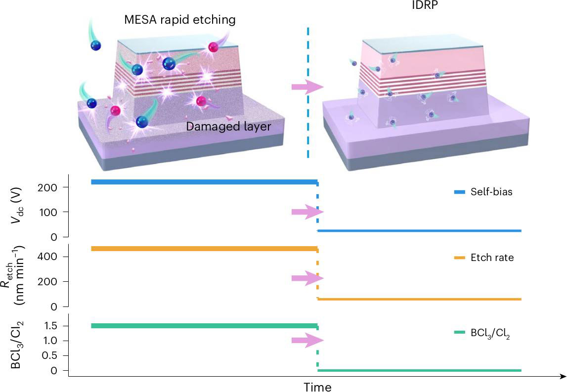
Figure 1: IDRP processing applied to mesa sidewall.
The IDRP process involved an ultra-low self-bias voltage, giving an ultra-low-energy chemical etch reaction to gently remove surface damage (Figure 1). In process optimization, the researchers found that pure chlorine (Cl2) plasma was preferable over the more usual mix with boron trichloride (BCl3).
The team comments: “While auxiliary gases such as BCl3 are sometimes used to reduce self-bias via charge neutralization between Cl anions and BClx cations, the auxiliary role of BClx ions in etching is mainly realized through physical bombardment of the surface, which is undesirable. Moreover, our first-principles calculations reveal that they are fundamentally detrimental to the sidewall’s electronic properties. Surface adsorption of B atoms introduces numerous deep-level electron traps within the bandgap, which facilitate non-radiative recombination. By contrast, Cl atom adsorption is benign, creating a beneficial conduction-band-localized barrier that passivates the surface by impeding electron flow without introducing harmful mid-gap states.”
High-angle annular dark-field scanning transmission electron microscopy (HAADF-STEM) showed the IDRP removed a 2–3nm amorphous layer from the BCl3/Cl2 ICP mesa etch. Beyond the amorphous layer lattice damage, the indium and aluminium elemental distributions in the light-emitting and electron-blocking layers was disrupted to depths of 50–100nm, as shown in energy-dispersive spectrometer (EDS) mapping.
The researchers comment: “This profound structural damage compromises the quantum confinement of carriers and critically degrades the EBL’s ability to prevent electron leakage. While these damages are confined to a limited depth near the sidewalls, their impact on carrier transport and recombination extends well beyond this region.”
The IDRP restored the integrity of the light-emitting indium gallium nitride (InGaN) multiple quantum wells (MQWs) and aluminium gallium nitride (AlGaN) electron-blocking layer (EBL) right up to the mesa perimeter. The process also removed boron and chlorine impurities from the mesa etch, leaving a surface passivation layer of adsorbed chlorine.
Micro-photoluminescence studies showed almost uniform emission, expanding the effective emission width in a 15μm ICP-etched mesa from 8.34μm before, to 14.81μm after the IDRP.
The researchers point out: “Crucially, the emission is enhanced not just at the periphery but across the entire mesa. The effect can be traced to the sidewall damage in the MQWs and EBL, which impacts carrier transport and recombination. This finding challenges the conventional view of damage being a purely localized effect and hints at a more complex carrier loss dynamic.”
Time-resolved studies of the photoluminescence showed a faster decay of the signal from the mesa before IDRP: 6.51ns at the edge, and 11.97ns at the center; to be compared with the after IDRP results of 12.29ns and 12.39ns, respectively.
The team reports: “This uniformity in recombination dynamics results in an overall improvement in the internal quantum efficiency (IQE). Intriguingly, although both devices exhibit similar carrier lifetimes at the centers, the IDRP-treated chip shows significantly higher emission intensity. This observation points to a crucial, previously under-appreciated loss mechanism: the damaged sidewalls act as powerful carrier ‘sinks’, inducing a concentration gradient that drives carriers from the ‘good’ central area to the periphery, where they are annihilated non-radiatively. This reduces the carrier density in the ‘good’ central area and dominates the observed decline in radiative emission.”
These carrier sinks are removed by IDRP.
The researchers also used capacitance−voltage measurements on planar metal/aluminium oxide/n-GaN capacitor structures to estimate interface trap density of mesas before IDRP at 1.03×10¹²/cm2-eV. After IDRP the trap density was below the detection limit of the method.
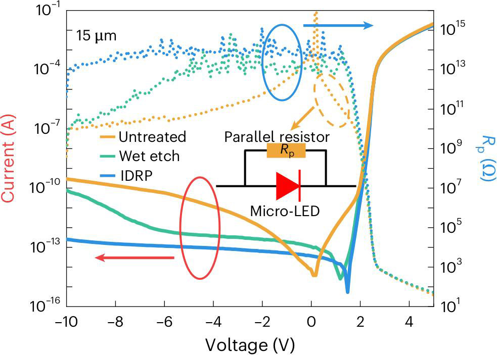
Figure 2: Current−voltage and parallel resistance (Rp) curves of 15μm micro-LED chips comparing different treatments.
The impact of IDRP relative to untreated and wet etch treatment LEDs was seen in much lower leakage currents revealed under reverse bias (Figure 2). The leakage at −5V was ultra-low in the IDRP sample at 1.02×10⁻¹³A, continuing low down to −10V.
Simulations of the structure suggested to the team that EBL damage was a second key contributor to the leakage beyond the InGaN MQW defects: “This damaged EBL creates a current ‘funnel’ at the sidewall, which concentrates current into the defective region, exacerbating both non-radiative recombination and electron overflow.”
IDRP repair also improved the 100% yield voltage in electrostatic discharge (ESD) tests from 200V to 270V.
The researchers comment: “By contrast, conventional wet etching, despite partially removing damage, actually degrades ESD performance. In addition, wet etching requires additional processing steps and increases fabrication cost. As device dimensions shrink, its anisotropic lateral etching becomes increasingly difficult to be controlled. This process produces rough and non-uniform sidewalls that compromise passivation integrity, ultimately reducing device uniformity and yield.”
The IDRP process managed to reverse the usual size tendency for external quantum efficiency of the LEDs (Figure 3). The peak EQE for 100μm blue LEDs based on IDRP mesas had peak EQEs of 38.9%, which increased to 47.6% for the smaller 1.6μm devices.
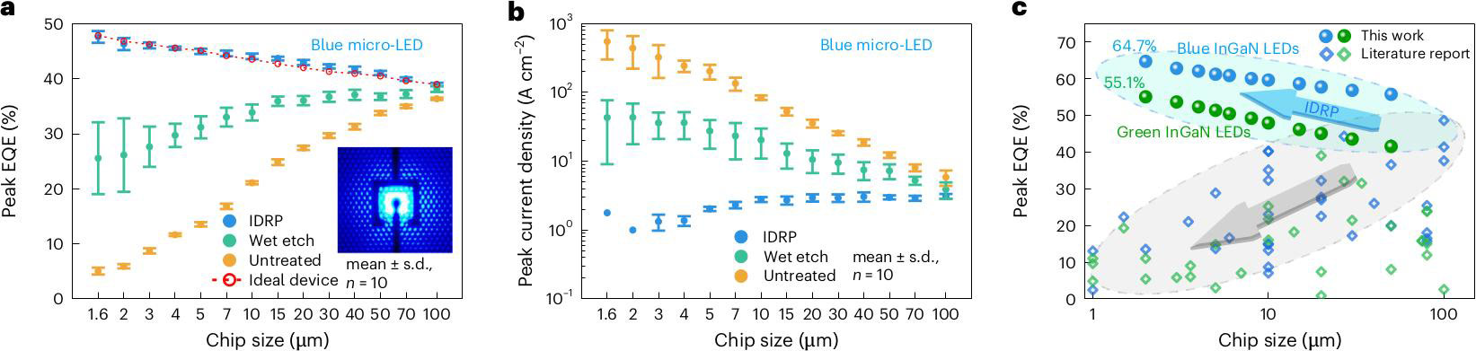
Figure 3: Peak EQE (a) and peak current density (b) of blue micro-LEDs showing mean ± standard d deviation over 10 randomly selected chips per size and process condition. (c) Peak EQE versus size relationship of InGaN-based micro-LEDs with integrated distributed Bragg reflectors (DBRs).
The researchers comment: “This occurs because IDRP has created nearly ‘ideal’ devices where the detrimental sidewall recombination is eliminated, and device performance becomes governed by the intrinsic physics of light-extraction efficiency, which is known to improve as device dimensions shrink.”
The 98.8% yield performance of IDRP devices is also seen as another critical advantage for manufacturing control. The yields for untreated and wet-treated LEDs were 90.5% and 75.0%, respectively.
Integrating DBRs into the IDRP LEDs supercharged the EQE performance to 64.7% for 2μm blue devices. Similar 2μm green LEDs also achieved an impressive improved 55.1% EQE.
The team explains: “Notably, these green devices exhibit a much stronger reversed size effect, with the peak EQE increasing from 41.5% at 50μm to 55.1% at 2μm. This enhanced effect is attributed to the poorer crystal quality and higher optical extinction coefficient of the high-indium-content material. In larger chips, photons undergo longer optical paths and are more likely to be lost to internal reabsorption; miniaturization dramatically reduces these losses, leading to a more significant LEE improvement compared with their blue counterparts.”
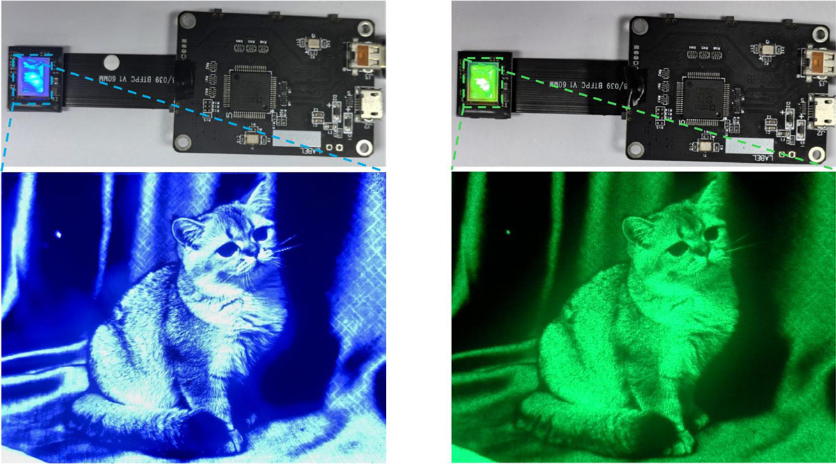
Figure 4: Blue (left) and green (right) monochrome 0.39-inch microdisplay modules with real-world displayed images. Corresponding ‘cat videos’ can be seen in blue and green.
The researchers further demonstrated the IDRP capability by fabricating high-pixel-density blue and green micro-LED arrays (Figure 4). The 0.39-inch 1,024x768 displays featured 3387pixels/inch (PPI) resolution. The individual pixels were based on 6.5μm LEDs at 7.5μm pitch.
Blue and green micron-scale LEDs AlGaN InGaN
https://doi.org/10.1038/s41566-026-01990-4
https://media.springernature.com
https://media.springernature.com/original
The author Mike Cooke is a freelance technology journalist who has worked in the semiconductor and advanced technology sectors since 1997.