

News: LEDs
10 September 2026
TMAH and passivation to boost external quantum efficiency
Researchers based in China report up to 363% improvement in external quantum efficiency (EQE) of 1–5μm indium gallium nitride (InGaN) light-emitting diodes (LEDs) through coupled tetra-methyl ammonium hydroxide (TMAH) treatment and dielectric passivation following plasma etch of the device mesa [Qin Wang et al, Appl. Phys. Lett., v129, p063309, 2026]. The effect was strongest for the smallest 1μm LED.
The team from the Beijing Key Laboratory for New Energy Materials and Devices, University of Chinese Academy of Sciences, and Songshan Lake Materials Laboratory, comments: “These findings validate the effectiveness of chemical etching coupled with dielectric passivation technology in micro-LED manufacturing, and also reveal the significant impact of sidewall defects in size-dependent efficiency.”
Micron-scale LEDs are being developed particularly with a view to high-resolution displays, as deployed for virtual/augmented-reality systems. However, such devices are much more prone to efficiency-sapping sidewall defects introduced in LED processing, particularly in the mesa-etch step. The ratio of the sidewall to device volume scales inversely with the device scale — i.e. the sidewall effect increases as the scale goes down.
The team explains: “This causes the sidewall damage layer induced by dry etching to become the primary non-radiative recombination pathway. This damage layer typically contains high-density point defects, dislocations, and dangling bonds, severely inhibiting carrier recombination efficiency and consequently reducing the internal quantum efficiency (IQE) and optical output power.”
Although TMAH on its own has been found to mitigate EQE degradation, it has limited ability in repairing deep-seated defects, according to the team. The researchers deployed a two-layer dielectric passivation to further improve EQE: atomic layer deposition (ALD) aluminium oxide (Al2O3) and plasma-enhanced chemical vapor deposition (PECVD) silicon dioxide (SiO2). The PECVD layer overcame the limited chemical saturation capability for deep-level defects of the ALD layer.
The researchers comment: “Compared to previous sidewall repair strategy, chemical etching removes the damage layer caused by dry etching and optimizes the sidewall morphology, while dielectric passivation ensures full saturation of the sidewall dangling bonds; the combination of these two processes effectively suppresses non-radiative recombination at the sidewalls.”
The researchers used a commercial epitaxial structure to fabricate their devices (Figure 1). The sequence of III-nitride layers was 3μm n-GaN, 100nm aluminium gallium nitride (n-AlGaN) electron-blocking layer, 200nm InGaN/GaN strain modulation, 150nm InGaN/GaN multiple quantum well (MQW), and 100nm p-GaN contact.
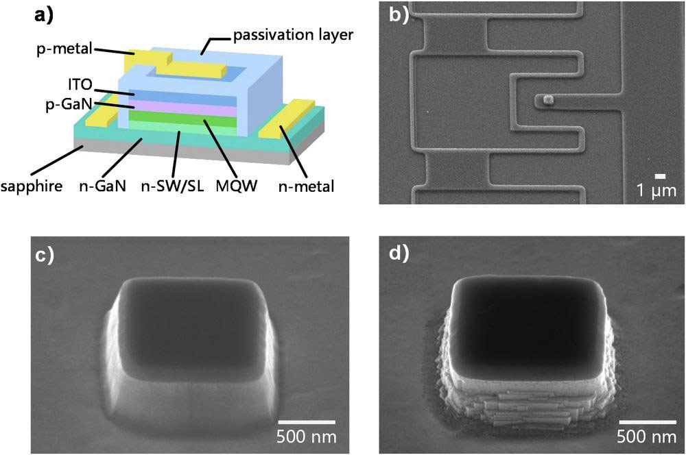
Figure 1: Forward-structured InGaN micro-LED. (a) Epitaxial layer and structure. (b) Scanning electron microscope (SEM) top view of 1μm device. SEMs of device mesa (c) without and with (d) coupled chemical etching.
The LED fabrication began with depositing 100nm of indium tin oxide (ITO) as a transparent conducting layer by magnetron sputtering. This was followed by 12 minutes of annealing at 550°C.
The device mesas were etched using inductively coupled plasma-reactive-ion etching (ICP-RIE). The dry etch damage was repaired by tetra-methyl ammonium hydroxide (TMAH) etch at 85°C for 3 minutes.
The passivation consisted of 50nm of ALD Al2O3 and 200nm of PECVD SiO2. The chromium/platinum/gold (Cr/Pt/Au) metal contacts were deposited through ICP-RIE windows in the passivation.
The TMAH treatment enabled much improved EQE and electrical performance (Figure 2). For the smallest 1μm LEDs, the peak EQE increased by 363% to 14.01% due to TMAH/passivation. For the 5μm LED the treatment increase was by 151% to 40.46% EQE.
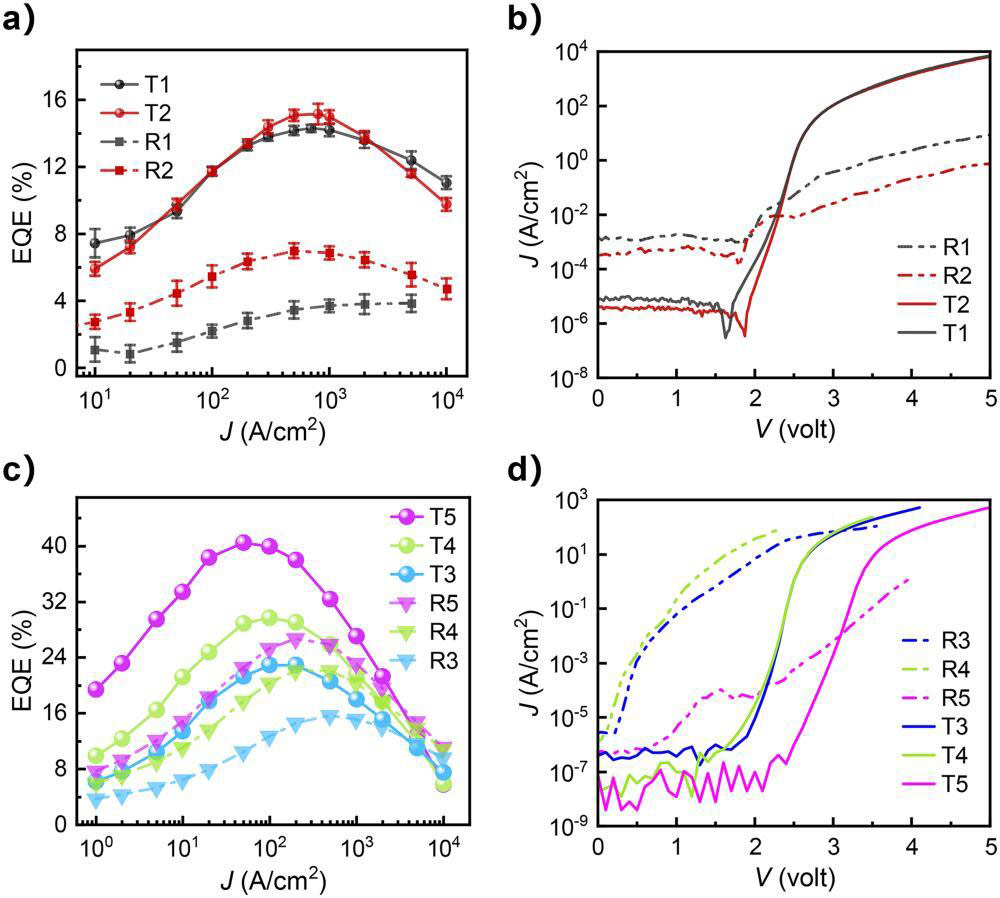
Figure 2: (a) External quantum efficiency (EQE) and (b) current density versus voltage (J–V) curves of 1μm and 2μm micro-LEDs before (R) and after (T) coupled chemical etching. (c) EQE and (d) J–V curves of 3–5μm micro-LEDs.
The graphs also show a 1–3 orders of magnitude decrease in the leakage current before turn on in all the devices after TMAH treatment, along with higher on/off current ratios. The effect was again strongest for the smallest devices.
https://doi.org/10.1063/5.0328266
The author Mike Cooke is a freelance technology journalist who has worked in the semiconductor and advanced technology sectors since 1997.