

News: Optoelectronics
21 October 2026
Photon Bridge raises €10m to tackle AI’s emerging laser bottleneck
Photonic integration firm Photon Bridge of Eindhoven, The Netherlands has raised €10m to tackle the emerging bottleneck in AI infrastructure: producing the millions of lasers that will be needed to connect increasingly large clusters of AI processors.
The round was co-led by European venture capital firms Amadeus APEX Technology Fund and 360 Capital as new investors, with existing investors Innovation Industries, Faber, and Brabant Development Agency (BOM) also increasing their investment.
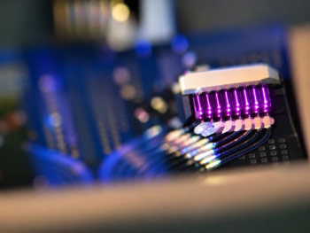 Picture: Photon Bridge’s external laser source prototype.
More than 20 million data-center AI accelerators are forecast to ship annually by 2028, according to Omdia. As AI clusters grow from thousands to hundreds of thousands of processors, moving data between those chips is becoming one of the fundamental constraints on their performance.
Goldman Sachs Research expects the rapid build-out of AI infrastructure and rising computing power per rack to expand the addressable market for optical networking ninefold to $154bn by 2028.
Since optical connections can move enormous amounts of data faster and more efficiently than conventional electrical interconnects, they are consequently moving progressively closer to the processors themselves. This shift is accelerating with the emergence of co-packaged optics, which integrates optical connectivity directly alongside the chips responsible for moving data through AI systems. But that creates another problem, notes Photon Bridge: the industry needs a vastly greater supply of the lasers that generate that light.
Today’s high-power laser supply chain was largely built for telecom and subsea networks, where volumes are far lower. AI could transform the laser from a specialist photonics component into something that has to be manufactured at semiconductor scale. Photon Bridge has designed its technology around that transition.
Rather than generating the required optical power using a small number of increasingly powerful lasers, Photon Bridge combines and multiplexes light from multiple lower-power semiconductor lasers.
Lower power densities make individual lasers less sensitive to manufacturing defects, improving production yield and allowing Photon Bridge’s architecture to scale more efficiently as volumes increase. The platform is designed to deliver high wavelength counts with up to 40mW of optical power per wavelength per fiber, while enabling high-volume production across multiple indium phosphide (InP) foundries.
“AI is fundamentally changing the way computing infrastructure is built,” says CEO Paul Marchal. “We are moving towards enormous systems in which hundreds of thousands of processors have to operate together, and moving data between them is becoming one of the defining constraints on performance. That means optics has to move closer to the compute. But it also creates an entirely different manufacturing challenge,” he adds. “The industry will soon need millions of these laser sources every year. Instead of making individual lasers increasingly powerful and difficult to manufacture, we move that scaling challenge into the architecture.”
Photon Bridge’s approach is designed around manufacturing yield, which is a consideration that becomes increasingly important as laser production moves from traditional telecom volumes towards the scale required by AI infrastructure.
“Every new wave of compute creates new bottlenecks further down the supply chain, and lasers are the next one,” notes Ion Hauer, investment partner at APEX Ventures. "Photon Bridge is addressing this with a technology that combines deep photonics expertise with a credible path towards manufacturing at very large scale,” he adds.
“AI is turning lasers from a telecom component into a semiconductor-scale product,” says Cesare Maifredi, partner at 360 Capital. “Once you start talking about millions of units a year, manufacturing yield becomes fundamental. Photon Bridge has designed its architecture from the beginning around the volumes this market is going to require.”
The financing will allow Photon Bridge to accelerate product development and customer qualification, deliver its first samples in 2027, and prepare for volume manufacturing from 2028. The firm will also expand its team in Eindhoven as it moves towards commercialization.
Photon Bridge and PHIX partner on DWDM external laser sources for hyperscale AI data centers
Photon Bridge and CPFC partner to validate path to scalable multi-wavelength light engines
Photon Bridge demos >30mW laser output per color at wafer scale on silicon photonics
Photon Bridge unveils integrated tunable laser PIC to power AI data-center interconnects