

News: Microelectronics
7 October 2026
Monolithic III-N complementary logic
Peking University and Hong Kong University of Science and Technology (HKUST) have reported a III−nitride-based complementary logic (CL) platform from the monolithic integration of polarization-doped indium gallium nitride (InGaN) p-channel field-effect transistors (p-FETs) and GaN n-FETs [Yu et al., Sci. Adv. v12, eaec4563, 2026].
Complementary logic is the basis for the widespread deployment of silicon semiconductor technology, based on features like low static power consumption. A bottleneck for achieving similar operation in the III−nitride system is the difficulty in gaining adequate hole concentrations and mobility. Normally, p-type conduction is obtained by doping with magnesium (Mg). Unfortunately, the high activation energy needed for accepting/grabbing electrons, and thus releasing holes, means that the doping efficiency is very low.
There has been increasing interest recently in using the contrasting charge polarizations of the III-nitride system to realize better p-type conduction. The charge polarization has spontaneous and strain-dependent (piezoelectric) components. The spontaneous polarization is related to the non-centrosymmetric crystal structure.
The Peking/HKUST team has used polarization-doping enhancement to claim a record maximum voltage gain of 154.1V/V, a state-of-the-art propagation delay of 10.4ns per stage for ring oscillators, the first implementation of a CL six-transistor static random access memory (6T-SRAM), and robust thermal stability of CL inverters up to 200°C.
The researchers also implemented power transistors alongside the CL circuitry with a view to next-generation high-frequency power management and harsh environment systems.
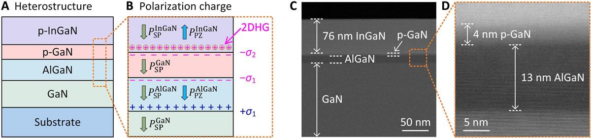
Figure 1: (A) Schematic structure and (B) polarization charge distribution of specially designed p-InGaN/p-GaN/AlGaN/GaN heterostructure. (C and D) Cross-sectional transmission electron microscope (TEM) images of heterostructure.
The CL devices used polarization charges to create a two-dimensional hole gas (2DHG) in the top p-InGaN of a p-InGaN/p-GaN/AlGaN/GaN metal-organic chemical vapor deposition (MOCVD) heterostructures on 2-inch sapphire (Figure 1). The doping of the p-type layers consisted of a nominal magnesium (Mg) concentration of 3×10¹⁹/cm3.
The sheet hole density of the 2DHG was estimated at 1.8×10¹³/cm2 from Hall measurements at 150K. As the temperature increased above 200K, a bulk hole conduction component from the Mg doping appeared, giving an extra contribution to the sheet hole density of around 0.64×10¹³/cm2 at room temperature (300K). The hole mobility decreased from 13.2cm2/V-s at 150K to 7.6cm2/V-s at 300K.
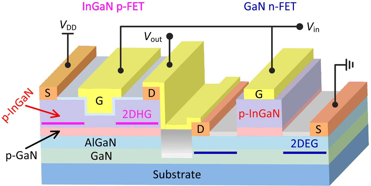
Figure 2: Schematic of CL inverter built on heterostructure.
Suitable fabrication enabled the formation of both p-FETs with 2DHGs at p-InGaN/p-GaN interfaces and n-FETs from 2DEGs at AlGaN/GaN interfaces (Figure 2).
The p-FETs were constructed with recessed gates, depleting the 2DHG underneath, enabling E-mode operation. The gate was separated from the p-GaN layer by around 20nm of p-InGaN. The gate length (LG) was 2μm, and the spacings of the gate and source/drain (LGS/LGD) were both 4μm.
For the E-mode n-FETs the p-InGaN/p-GaN was fully removed by etching the material above the AlGaN/GaN layer, forming a 2DEG, except in the p-InGaN/p-GaN gate stack region. The AlGaN surface was passivated with 50nm silicon dioxide. The LGS/LG/LGD sequence was 3/5/3μm.
The researchers adopted a theoretically optimal gate width ratio of 1:10 to respectively balance the GaN n-FET and InGaN p-FET performances.
Table 1: Static characteristics.
Device |
Threshold (VTH) | Subthreshold swing (SS) | ON/OFF current ratio (ION/IOFF) | On-resistance (RON) | Maximum current density (Imax) |
| p-FET | −2.2V | 114mV/decade | 1.46×10⁸ | 0.65kΩ-mm | −20.4mA/mm |
| n-FET | +1.2V | 108mV/decade | 2.11×10⁹ | 6.9Ω-mm | 350mA/mm |
The large p-FET ION/IOFF (Table 1) was enabled by an ultralow leakage current arising from strong gate control, and minimal gate leakage due to high-quality silicon nitride (SiN) gate dielectric. Low leakage is critical for low static power consumption in CL applications. The n-FET performance was typical for such GaN transistors with p-GaN gate structure.
In particular, the researchers compared their p-FET performance with state-of-the-art planar-gate GaN p-FETs (Figure 3).
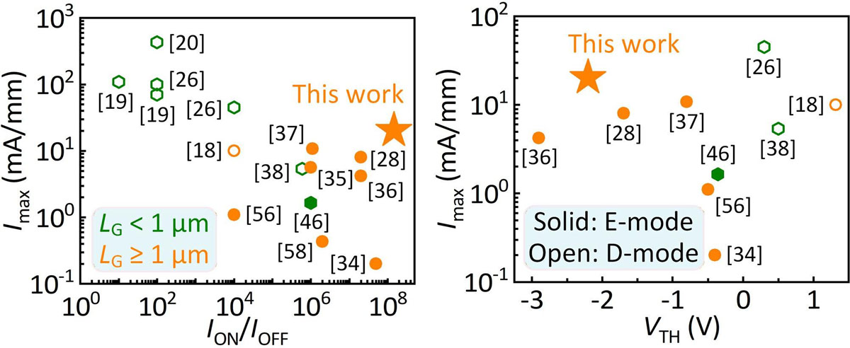
Figure 3. Benchmarks of InGaN p-FET against state-of-the-art planar-gate GaN p-FETs, comparing Imax versus (left) ION/IOFF and (right) VTH.
The researchers demonstrated a series of III−nitride CL building blocks, including inverter, ring oscillator (RO), NAND gate, NOR gate, RS latch, and six-transistor static random-access memory (6T-SRAM). The inverter achieved a record maximum voltage gain of 154V/V.
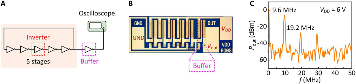
Figure 4: (A) Circuit schematic diagram and (B) microscopic image of 5-stage ring oscillator (RO). (C) Power spectrum of 5-stage RO.
A 5-stage ring oscillator circuit based on the CL inverter platform achieved a record short propagation delay per stage (τpd = 1/2Nfosc, N = 5) of 10.4ns (Figure 4). The circuit consisted of 5 inverters cascaded into a ring with an additional inverter serving as output buffer. This buffer isolated the oscillation core from the large parasitic capacitance of the external testing environment. The fundamental frequency (fosc) was 9.6MHz.
The researchers also claim the first realization of GaN-based CL 6T-SRAM, and report: “The read and write margins of the CL 6T-SRAM were characterized under a supply (VDD) of 6V. During the read operation, with the word-line (WL) set to 3V, the read margin is measured at 1.23V. A stable write operation for the 6T-SRAM is also observed when the WL is set to 6V, yielding a write margin of 1.48V.”
By extending the gate-drain distance to 15μm, the researchers could implement CL and power E-mode HEMTs monolithic circuits (Figure 5). The power transistor gate width was 100μm. The resulting power transistor had a 1394V breakdown voltage at 1μA/mm drain leakage. A monolithically integrated circuit of III−nitride CL buffers and GaN power HEMT demonstrated the proper switching operation of the GaN power HEMT.
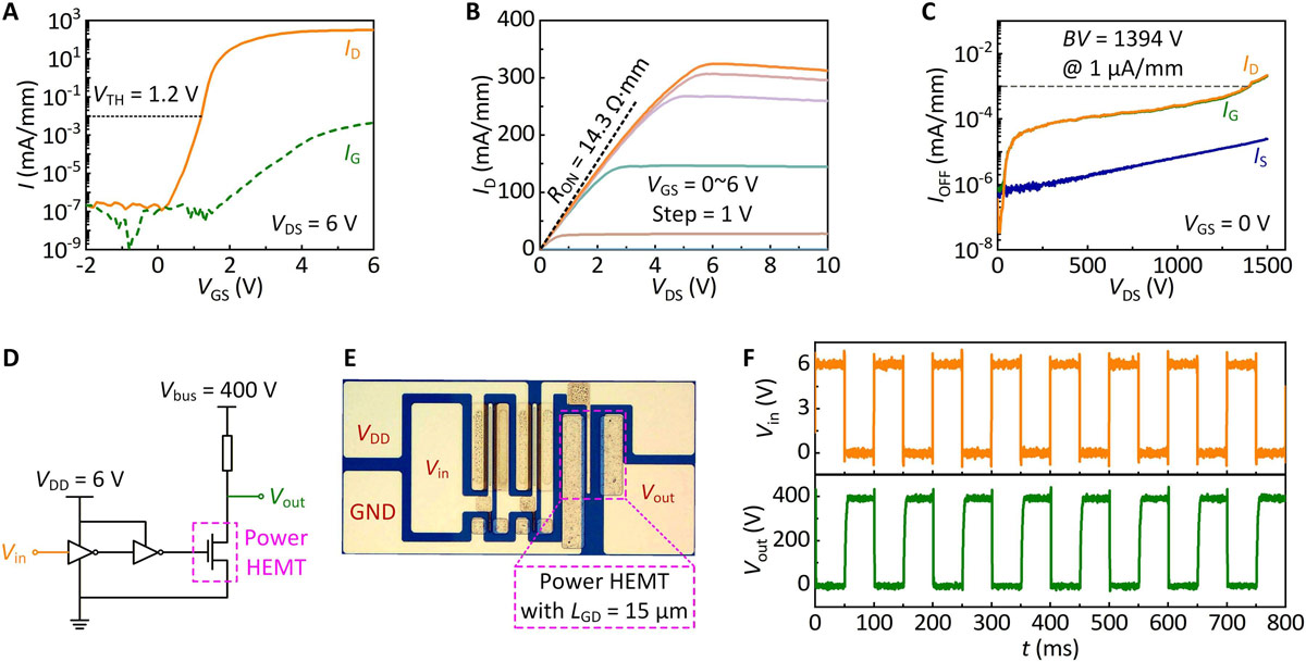
Figure 5: (A) Transfer characteristics of E-mode GaN power HEMT. (B) Output characteristics. (C) OFF-state leakage current characteristics of the GaN power HEMT at VGS = 0V. (D) Circuit schematic diagram and (E) microscopic image of monolithically integrated III-nitride CL buffers and GaN power HEMT. (F) Input and output waveforms with 6V logic supply and bus voltage of 400V.
Comparing their platform with previously reported work on CL GaN circuits, the team comments: “Our CL inverter demonstrates significant improvements in logic swing, noise margins, and voltage gain — achieving a record maximum voltage gain of 154.1V/V.”
Complementary logic InGaN p-FETs GaN n-FETs MOCVD
https://doi.org/10.1126/sciadv.aec4563
The author Mike Cooke is a freelance technology journalist who has worked in the semiconductor and advanced technology sectors since 1997.