

News: LEDs
5 November 2026
Top-emitting efficient deep ultraviolet LEDs
Japan’s National Institute of Information and Communications Technology (NICT) has reported 275nm deep ultraviolet (DUV) top-emitting aluminium gallium nitride (AlGaN) light-emitting diodes (LEDs) with 7.5% external quantum efficiency (EQE) and 6.5% wall-plug efficiency (WPE) [Guo-Dong Hao et al, ACS Photonics, online 21 October 2026].
The researchers comment: “This work provides the first demonstration of top-emitting AlGaN-based DUV LEDs, confirming the feasibility of fabricating top-emitting DUV LEDs and providing a pathway toward low-cost and high-efficiency devices.”
DUV devices are being developed with a view to surface disinfection, air and water purification, food safety, photolithography, ultraviolet curing, and solar blind communications.
AlGaN DUV LEDs suffer from a number of factors that limit efficiency. One challenge is that the p-side of the device typically contains a final p-GaN layer rather than p-AlGaN, in order to generate enough holes to inject into the light-emitting region. But p-GaN heavily absorbs DUV light, so any radiation emerging is largely from the back side of chip, i.e. through the substrate. Such devices need to be flipped and contacted to a submount, a tricky fabrication process.
The researchers comment: “Top-emitting DUV LEDs offer advantages that can overcome these issues. Because this configuration does not require a submount, the fabrication process is simplified and production costs can be reduced by eliminating the chip transfer step. In addition, the light generated in the AlGaN active region can be directly extracted without passing through the substrate.”
The researchers used AlGaN of various compositions, including a light-emitting multiple quantum well (MQW), electron-blocking layer (EBL), and cladding (Figure 1). The top cap layer consisted of p-GaN.
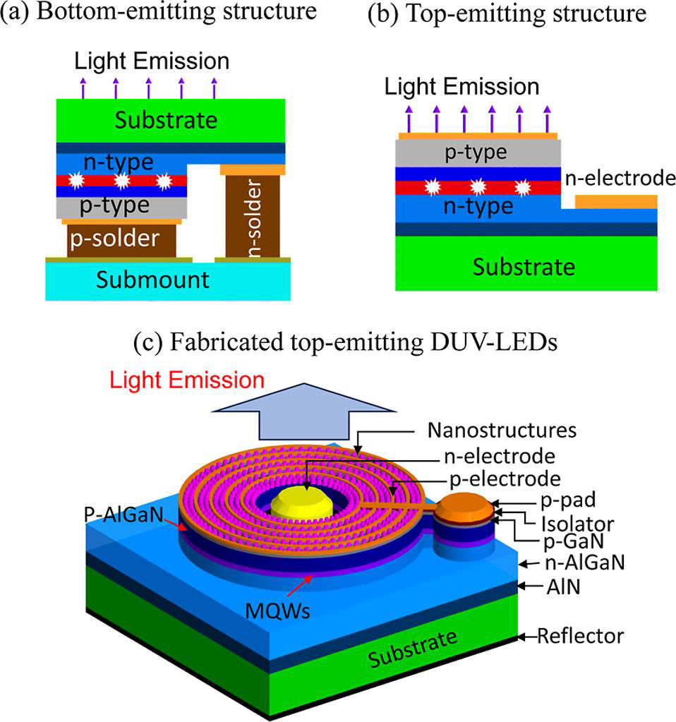
Figure 1: (a) Conventional bottom-emitting flip-chip DUV-LED structure, (b) top-emitting DUV-LED structure, and (c) NICT’s top-emitting DUV-LED configuration.
The fabricated LED included a bottom reflector of aluminium deposited on the back side of the sapphire substrate. The device mesa consisted of a circular ring with inner and outer diameters of 200μm and 600μm, respectively.
The p-electrodes consisted of concentric rings of metal 2μm wide, placed at 10μm pitch, covering around one-fifth of the mesa area. The regions between the electrodes were etched down to the p-AlGaN and filled with nano-structured hafnium dioxide (HfO2). The etching was performed at low bias power to reduce plasma damage. The HfO2 was deposited by RF magnetron sputtering, and patterned into truncated cones designed to enable the UV to emerge from the device without being reflected back into the device, enhancing light extraction efficiency (LEE).
The n-electrode was placed within the central part of the ring-mesa. The LEDs were packaged as encapsulated 1mm x 1mm chips.
The researchers point out that the central position of the n-electrode is unusual — normally a circular LED has the n-electrode as a ring of metal outside the device mesa.
The ring mesa design reduces the distance that laterally guided light travels before extraction from the inner and outer sidewalls.
The team comments: “This enables photons to be extracted with fewer reflections, thereby decreasing the amount of light absorbed by the p-electrode. Furthermore, placing the n-electrode at the center rather than around the outer edge of the mesa minimizes the light absorption by the n-electrode when the guided light laterally propagates toward the chip edge via multiple reflections, thus enhancing the light-extraction efficiency.”
At low current levels, less than 50mA, the light intensity enhancement over the performance of the same device structure in a flip-chip configuration was 1.35x. When the HfO2 was not nano-textured with truncated cones there was still an enhancement of 1.13x.
At 200mA, the enhancement reached 2.1x, due to suppression of the efficiency droop that is typically seen at higher currents.
The researchers comment: “This improvement in the efficiency droop is ascribed to reduced self-heating, as confirmed by the comparison under pulsed current injection (Figure 4b), which excludes the thermal influence.”
The higher wall-plug efficiency reduces heating, since more of the input power is converted to light rather than heat. Also, the devices had improved thermal management to better dissipate any generated heat.
The team reports: “In the top-emitting DUV LED, the entire substrate (1mm2) is in direct contact with the TO-can, providing a much larger heat dissipation contact area than that of the flip-chip DUV LED, in which heat is dissipated only through the n- and p-pads (0.06mm2) connected to the submount to avoid current leakage due to solder flow.”
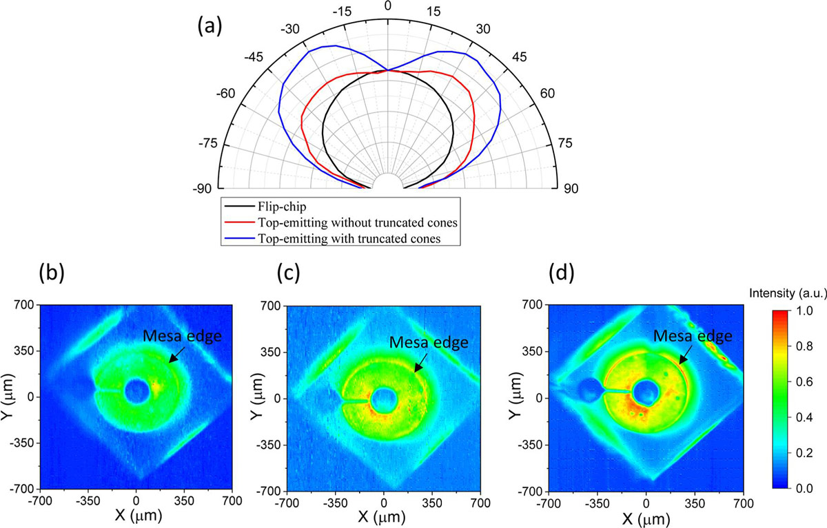
Figure 2: (a) Far-field patterns for three DUV LEDs and near-field pattern for (b) conventional flip-chip DUV LEDs, (c) top-emitting DUV-LEDs, and (d) top-emitting DUV LEDs incorporating HfO2 truncated cones.
The devices with truncated cone texturing showed strong emission at about 40° to the normal (Figure 2). The researchers explain: “Electromagnetic wave propagation simulations suggest that these light-extraction efficiency enhancements originate from the combined effects of an enlarged light escape cone and reduced Fresnel reflection.”
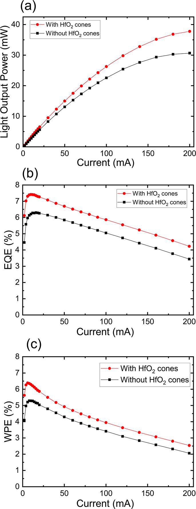
Figure 3: (a) Light output power, (b) EQE, and (c) WPE for top-emitting DUV LEDs with and without HfO2 nanostructures.
The devices with HfO2 nanostructuring achieved 38mW light output at 200mA injection (Figure 3). The peak external quantum efficiency (EQE) was 7.5% at 10mA injection; the wall-plug efficiency was 6.5% at 7mA.
https://doi.org/10.1021/acsphotonics.6c00589
The author Mike Cooke is a freelance technology journalist who has worked in the semiconductor and advanced technology sectors since 1997.