


News: LEDs
14 May 2026
Red InGaN micro-LEDs with narrow FWHM and high EQE
University of Michigan in the USA has claimed the highest external quantum efficiency (EQE) and smallest linewidth so far for red-emitting indium gallium nitride (InGaN) micro-LEDs, using photonic crystal (PhC) structures [Yuanpeng Wu et al, Light: Science & Applications v15, p133, 2026]
Further, the emission wavelength was stable for a wide range of injection currents. The 5nm full-width at half maximum (FWHM) was about one order of magnitude narrower than previously reported values.
The researchers see narrow linewidths as “paramount for achieving high color purity”.
The InGaN family of semiconductor alloys has a wide range of potential emission wavelengths. As the indium content increases, however, the device efficiency tends to deteriorate. High indium fractions are needed for longer red wavelengths, impeding development of full-color InGaN micro-LED arrays.
The team explains: “While the EQE of blue and green InGaN micro-LEDs has increased significantly, the EQE of micrometer-scale red InGaN micro-LED is well below 1%, and few groups have reported several percent EQE values, which can be mainly attributed to the high densities of defects and dislocations in high-indium-composition InGaN quantum wells (QW).”
The Michigan devices could lead to “monolithic integration of GaN-based RGB-pixelated micro-LEDs with CMOS-based driver circuitry.”
The researchers comment: “The near-diffraction-limited emission area and ability to form large, ordered arrays make them highly promising for ultra-high-resolution micro-displays in augmented/virtual/mixed reality. The narrow-linewidth emission and directionality of the photonic band-edge modes are advantageous for visible-light communication, wherein the reduced spectral crosstalk and high modulation bandwidth expected from nanoscale emitters could support high-speed, low-latency optical data links in next-generation wireless systems.”
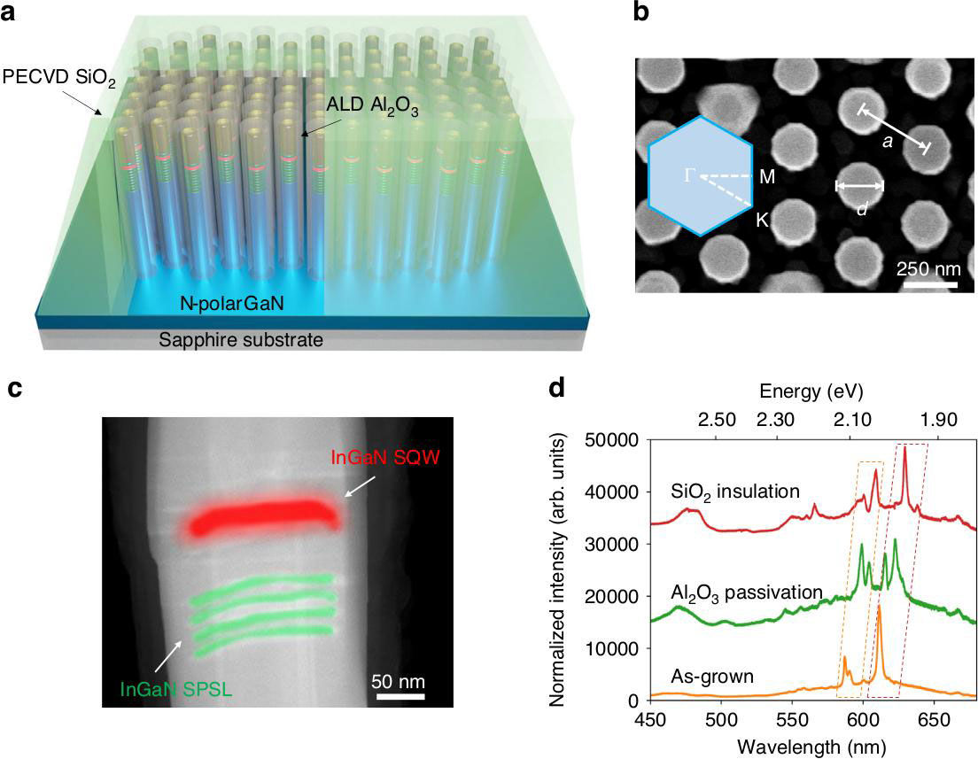
Figure 1: a InGaN/GaN nanowire array scheme in photonic crystal structure. b Top view scanning electron microscope (SEM) image of as-grown InGaN/GaN PhC structure, and (inset) corresponding reciprocal lattice. c Cross-sectional false-color scanning transmission electron microscope (STEM) image of active region. d Photoluminescence spectra from sample as-grown (orange), after Al2O3 passivation (green) and SiO2 deposition (red). Evolution of photonic crystal mode indicated by dashed rectangles.
The photonic crystal (PhC) structure consisted of a hexagonal/triangular array of vertical III-nitride 220nm-diameter nanowires grown from a N-polar GaN/sapphire substrate using a 10nm titanium mask (Figure 1). The nanowires included a red single quantum well (SQW) of InGaN grown on top of an InGaN short-period superlattice (SPSL). The SPSL released the strain between GaN and InGaN, enabling better indium incorporation in the SQW: around 36% on the c-plane and 40% on the semi-polar plane near the edges of the nanowires. The lattice constant (a) of the hexagonal array was 360nm.
The researchers found a dominant photoluminescence (PL) peak at 612nm with a 3nm FWHM, attributed to the Γ1 band-edge mode of the PhC. Other modes resulted in lesser peaks at 587nm and 591nm.
Surface passivation with 10nm atomic layer deposition (ALD) aluminium oxide (Al2O3) split the dominant peak into two, at 616nm and 623nm. The two shorter wavelengths shifted to 599nm and 604nm. Further shifts were seen with plasma-enhanced chemical vapor deposition (PECVD) of 300nm silicon dioxide (SiO2) for electrical insulation: to 629nm for the dominant peak.
The researchers comment: “Such a shift can be attributed to the variation of the refractive index distribution, wherein the presence of the SiO2 increases the average background refractive index.”
Variation of the PL excitation power between 80mW/cm2 and 14.8W/cm2 showed negligible shift in the peak positions. The team points out that this “is in direct contrast to the significant blue-shift of 20–50nm observed in conventional red InGaN LEDs due to the screening of the quantum-confined Stark effect. The excited carriers within the InGaN SQW generate spontaneous emission coupled to the photonic band-edge mode of the PhC structure, wherein the emission wavelength is insensitive to the carrier density, and a negligible shift in peak wavelength is obtained.”
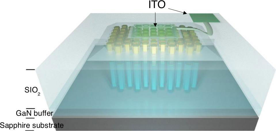
Figure 2: Micro-LED device structure.
The researchers fabricated the PhC arrays into micro-LEDs (Figure 2). The p-contact window consisted of indium tin oxide (ITO) transparent conducting material. The n-contact metal was titanium/gold.
The electroluminescence response from a device with a 5μmx5μm window showed a peak emission around 617nm with 5nm FWHM (Figure 3). The peak position did not vary under injection current densities ranging between 1.6A/cm2 and 52.8A/cm2. The chromaticity coordinate of the red-emitting micro-LED was (0.67, 0.33).
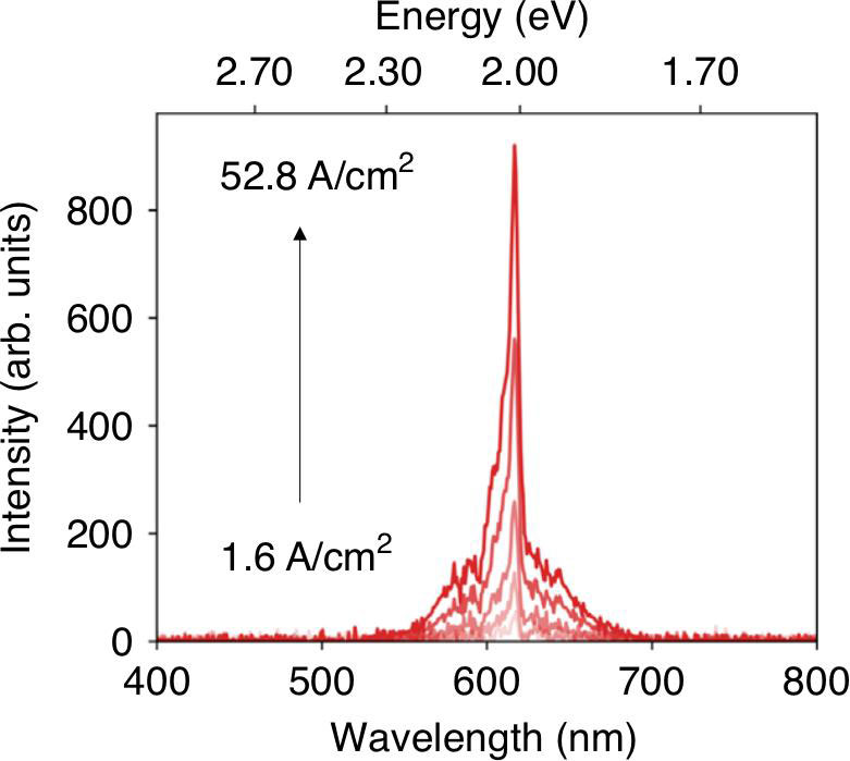
Figure 3: Current-dependent EL spectra for the micro-LED.
The researchers comment: “This coordinate coincides with that of the primary red color in the widely used National Television Standards Committee (NTSC) standard and is beyond the color gamut area of the Adobe RGB. In previously reported InGaN red-emitting micro-LEDs, while excellent color purity can be achieved at low current densities of a few A/cm2, the chromaticity coordinates deviate from the red region, and the color gamut coverage reduces due to the significant blue-shift with injection current.”
The peak EQE reached 12% at 4A/cm2 (Figure 4) when the devices were subjected to further fabrication with deposition of an aluminium/titanium/gold mirror on the ITO current-injection window region.
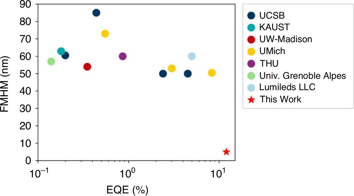
Figure 4: Benchmark of EQE and linewidth values for previously reported InGaN-based red micro-LEDs with device areas less than 400μm2.
The team explains the high EQE: “Directional emissions primarily along the vertical direction of the nanowire PhC structure were measured, which effectively improved the light-extraction efficiency.”
https://doi.org/10.1038/s41377-026-02227-3
The author Mike Cooke is a freelance technology journalist who has worked in the semiconductor and advanced technology sectors since 1997.


