


News: Optoelectronics
13 March 2026
TNO and High Tech Campus Eindhoven begin construction of first 6-inch indium phosphide photonic chip foundry
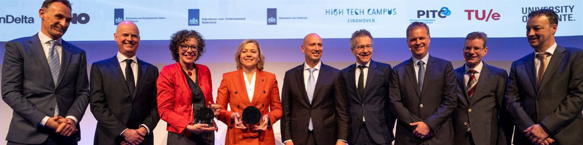
The research institute TNO (the Netherlands Organization for Applied Scientific Research in Delft) and High Tech Campus Eindhoven are starting construction of what is reckoned will be the world’s first foundry for producing indium phosphide photonic chips on 6-inch wafers. The official opening was attended by European Commission executive vice-president Henna Virkkunen and the Netherlands’ Minister of Economic Affairs and Climate Heleen Herbert, and Minister of Defence Dilan Yeşilgöz-Zegerius.
By connecting R&D with scalable production, the facility is expected to accelerate the path from concept to concrete market-ready solutions, paving the way for a new generation of energy-efficient AI data centers, 6G networks, medical innovations and supercomputers.
Critical link between ‘lab and fab’
The new facility aims to be a national and European catalyst for innovation. As demand for photonic chips grows exponentially, TNO says it is offering a critical function in the ecosystem by providing the infrastructure needed to safely test and validate the technology at industrial scale.
“For the first time, we are building an industrial pilot line,” says TNO’s CEO Tjark Tjin-A-Tsoi. “By bringing research and manufacturing closer together, we strengthen the Netherlands’ position within the European semiconductor landscape and help companies scale up high-quality photonic technology more quickly and efficiently. This is an investment in our technological strength and in future economic growth.”
Strategic autonomy for Europe
The €150m investment directly stems from the ambition of the European Chips Act. As part of the pan-European consortium PIXEurope, the factory aims to ensure that the ‘brains’ of the future digital economy are developed and produced on European soil.
“With this investment, we are moving from knowledge and innovation to concrete applications of integrated photonics,” comments Minister Heleen Herbert (Economic Affairs and Climate). “Our goal is to achieve a strong European competitive position with this key technology — in knowledge, innovation, supply chains, and end production. This is essential for future Dutch jobs and income, for solving societal challenges, and for our national security,” she adds.
Collaboration and employment
The project is a public-private partnership between TNO, TU/e, PhotonDelta, SMART Photonics, and High Tech Campus Eindhoven. In addition to technological progress, the factory should immediately create high-quality jobs. After the initial ramp-up phase, around 40 specialists will be employed, a number expected to grow further.
The impact of integrated photonics is comparable to the rise of integrated electronics decades ago, reckons government adviser Peter Wennink. “By investing now in scalable production capacity, we are creating an ecosystem that can help shape the global technological direction. This is a launchpad for Europe’s future digital economy.”
TNO to construct InP-based photonic chip pilot manufacturing line
imec and TNO launch Holst Centre Photonics Lab
Chips JU to fund new European pilot line for Advanced Photonic Integrated Circuits


