


News: Microelectronics
26 March 2026
Single- and multi-channel AlScN barriers
Cornell University in the USA claims the lowest sheet resistance so far for gallium nitride (GaN) single- and multi-channel heterostructures with aluminium scandium nitride (AlScN) barriers [Aias Asteris et al, J. Appl. Phys., v139, p075708, 2026].
The researchers see their work as contributing to next-generation high-speed, high-power GaN-based electronics. At low temperature the sheet resistance was even lower (around 3x), which may “enable new cryogenic devices, such as low-insertion-loss RF switches”.
Multi-channel structures can be fabricated into fin or gate-all-around field effect transistors (FETs).
The researchers used molecular beam epitaxy (MBE) on 7mmx7mm semi-insulating metal-polar GaN-on-sapphire template coupons to grow AlScN/GaN heterostructures. The GaN buffer layer was grown with the substrate at 575°C temperature and 1.7x10⁻⁷Torr pressure with a Ga-rich condition. Single- and multi-channel structures were developed. The single-channel stack consisted of a 400nm GaN buffer, AlN and GaN interlayers, and AlScN barrier. The structure was capped with 2nm GaN to protect the AlScN from degradation, since material containing aluminium tends to oxidize.
A two-dimensional electron gas was expected from simulations to form under the AlN due to band bending near the buffer/AlN interface. The thicknesses of the AlN and AlScN were designed to be strain balanced to the underlying GaN crystal lattice. AlN is tensile strained, and AlScN provides a compressive counter-balance. The researchers comment that there is “substantial variation in reported lattice-matching conditions between AlScN and GaN, with scandium concentrations ranging from 9% to 20% across different studies.”
A further limitation is that AlScN tends to form in mixed phases when the Sc content exceeds 25%. Also, the 2DEG carrier concentration tends to decrease with high-Sc-content barriers. This increases sheet resistance.
The purpose of the GaN interlayer was to increase the distance from the AlScN without too rapidly increasing the 2DEG density induced by a thicker AlN interlayer. Once 2DEG densities become too large the mobility, which measures the ability of electric fields to move carriers, decreases in a way that increases net sheet resistance.
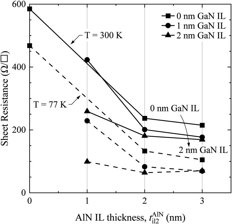
Figure 1: Experimental sheet resistance of single-channel Al0.88Sc0.12N/GaN heterostructures at 300K (solid) and 77K (dashed) with assorted interlayer (IL) configurations.
A range of interlayer and barrier thicknesses were studied at room temperature (300K) and cryogenic (77K) temperature (Figure 1). The lowest sheet resistance, 169Ω/□, was measured with 3nm AlN and 2nm GaN interlayers and 6nm AlScN barrier. The 2DEG density and mobility were 3.88x10¹³/cm2 and 951cm2cm/V-s, respectively.
Reducing the GaN/AlN interlayer thicknesses to 1nm/3nm and 2nm/2nm increased the resistance to 177Ω/□ and 181Ω/□, respectively. The 1nm/3nm combination reduced the 2DEG density to 3.74x10¹³/cm2, and the mobility to 946cm2cm/V-s. The 2nm/2nm managed to increase the mobility to 1370cm2cm/V-s, but at the cost of significantly reduced 2DEG density, 2.52x10¹³/cm2.
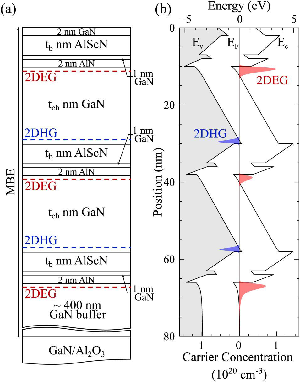
Figure 2: (a) Cross-sectional schematic and (b) simulated energy band diagram of multi-channel AlScN/GaN heterostructure.
With a view to reducing sheet resistances further, the researchers explored multi-channel structures with 1nm/2nm GaN/AlN interlayers (Figure 2).
The team comments: “Multi-channel realization requires minimal strain to preserve a pseudomorphic structure, which may be hindered by sequential AlN layers due to significant strain energy accumulation. While strain balance can minimize this accumulation, it demands thicker AlScN barriers of higher Sc content for thicker AlN interlayers. There are risks, however, associated with thick high-Sc AlScN layers, which include pronounced surface roughening due to growth under nitrogen-rich conditions, poor field management due to increased charge density, as well as complicated device fabrication due to increased stack thickness.”
The researchers studied AlScN barriers with thicknesses in the range 5–10nm, and 12–18% Sc content. Hall-effect measurements showed n-type conductivity with carrier densities reaching 8.90x10¹³/cm2 with 5-periods of 5nm AlScN barriers at 18% Sc content. The GaN channel layers were 40nm. The sheet resistance was 45Ω/□, and the mobility was 1550cm2cm/V-s.
The researchers found no evidence for the parallel two-dimensional hole gases (2DHGs) predicted by their energy-band simulations. The team comments: “If present, 2DHGs are likely masked by 2DEGs due to the significantly higher mobility of the latter compared to the former. Unbalanced electron and hole charge densities can also hinder the detection of 2DHGs.”
The team points out that 2DHGs “constitute parasitic parallel conduction channels and can degrade device performance. Their formation can be prevented via intentional donor doping, which enables precise control over 2DEG and 2DHG densities, and in turn device miniaturization.
The choice of structure for use in devices would need to be optimized for the application. Thinner structures can be favored for improved electrostatic control via gate structures in high-speed deployments. Thicker structures may offer improved conductivity/on-resistance for power applications.
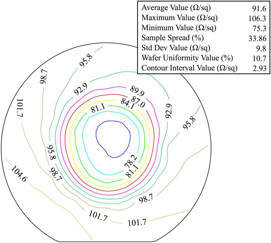
Figure 3: Sheet resistance for three-channel 5nm/1nm/2nm/40nm AlScN/GaN/AlN/GaN heterostructure grown on a 50mm wafer.
With a view to manufacturing the researchers grew a heterostructure on a 50mm-diameter GaN/sapphire template, rather than the 7mmx7mm coupons, and report the sheet resistance (Figure 3). The team comments: “The high uniformity over the growth surface indicates the ability for upward scaling of multi-channel AlScN/GaN heterostructures.”
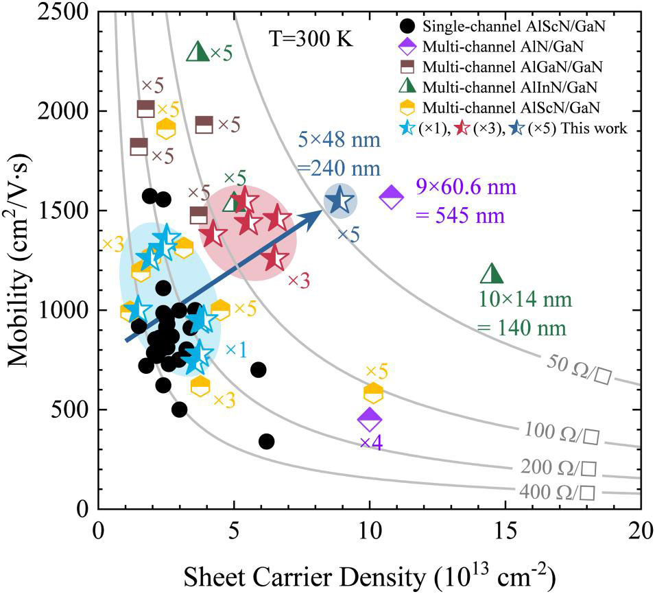
Figure 4: Benchmark of room-temperature Hall data for single- and multi-channel AlScN/GaN heterostructures against previous reports of GaN-based schemes.
The Cornell work puts the AlScN structure sheet resistance near to those of AlN/GaN (36Ω/□) and AlInN/GaN reports (Figure 4), state-of-the-art multi-channel III–nitride systems.
https://doi.org/10.1063/5.0312252
The author Mike Cooke is a freelance technology journalist who has worked in the semiconductor and advanced technology sectors since 1997.


