


News: Microelectronics
23 June 2026
Increasing passivated AlGaN power
University of Wisconsin-Madison in the USA reports passivated aluminium gallium nitride metal-insulator-semiconductor high-electron-mobility transistors (MISHEMTs) on sapphire with 1.7x the Baliga figure of merit (BFOM) of state-of-the-art passivated AlGaN-channel transistors on sapphire [Khush Gohel et al, physica status solidi (RRL)– Rapid Research Letters, 20:e70190, 2026].
The highest BFOM obtained was 325MW/cm2, with a breakdown voltage of 2.6kV. Although higher breakdowns can be achieved in unpassivated devices, the lack of passivation impacts dynamic performance.
The team comments: “Power electronics applications require devices that achieve both strong ON-state and OFF-state performance, necessitating effective surface passivation and optimized electric-field spreading.”
The researchers see aluminium-rich AlGaN on sapphire as potentially providing the needed high-field capabilities on a more scalable and cost-effective substrate platform compared with competing ultra-wide-bandgap (UWBG) semiconductor materials.
While other substrates could deliver higher performance, sapphire has the most long-established supply chain for III–nitride manufacturing, providing lower costs than most alternatives, while maintaining a dependable pathway for scalable device fabrication.
The researchers used metal-organic chemical vapor deposition (MOCVD) on AlN/sapphire templates to prepare the epitaxial material for the HEMTs (Figure 1). A thin 1nm AlN layer was placed between the channel and barrier AlGaN layers to improve the two-dimensional electron gas (2DEG) performance. Van der Pauw geometry Hall measurements gave 1.1×10¹³/cm2 as the 2DEG carrier concentration with 167cm2/V-s mobility.
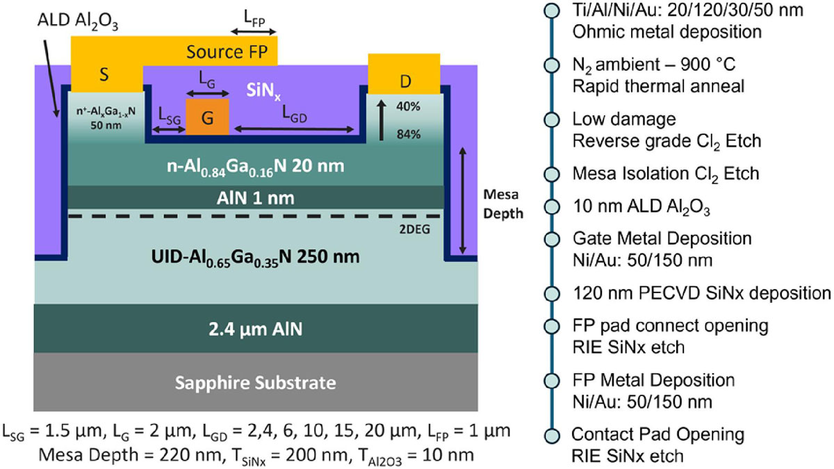
Figure 1: Left: Two-dimensional schematic (not-to-scale) of AlGaN-channel HEMT with source field plate. Right: fabrication flow.
The top AlGaN material was graded down to 40% Al to enable low-resistance ohmic contact with the annealed titanium/aluminium/nickel/gold metal source/drain electrodes.
After the electrode formation the gate and access regions were etched with a low-power chlorine-based reactive ion etch (RIE). The low power minimized the surface damage from the plasma. RIE to a depth of 220nm was also used for mesa isolation.
The gate dielectric was 10nm atomic layer deposition (ALD) aluminium oxide (Al2O3). The gate metals were nickel/gold.
Passivation was provided by 200nm plasma-enhanced chemical vapor deposition (PECVD) silicon nitride (SiNx). A source field-plate (FP) was added, measuring 1μm.
While the gate-drain distance (LGD) of the drift region was varied, the other dimensions were fixed: gate length (LG), 2μm; gate width, 100μm; and, source-gate spacing (LSG), 1.5μm. Longer drift regions spread the potential drop over a greater distance, reducing the peak electric field, and increasing breakdown voltages. However, this increases the resistance to current flow in the ON state.
The variation of the ON-resistance with LGD suggested an effective sheet resistance of 3477Ω/□, consistent with the 3100Ω/□ value from the standard transfer length method (TLM) measurements.
The researchers comment: “The observed deviation is attributed primarily to process-induced device variation, which becomes more pronounced at larger LGD.”
In pulsed operation a 15μm LGD device suffered a 10% increase in ON-resistance. The team reports: “Additionally, a reduction in maximum drain current from 273mA/mm (DC) to 235mA/mm is observed, along with a noticeable knee voltage walkout in the triode region. These effects indicate degradation in channel and access region conductivity under pulsed conditions This behavior is attributed to trapping effects, likely associated with surface and interface states, which modulate the charge distribution in the channel following OFF-state bias stress.”
The 15μm device had a voltage threshold of −12V at 0.1A/mm drain current. The ON/OFF current ratio was of order 106 at 30V drain bias. The device operation was stable up to near breakdown, which “suggests good dielectric integrity,” according to the researchers.
The researchers studied the breakdown characteristics in the OFF state (Figure 2). The average electric breakdown field was estimated from the breakdown voltage (BV) by BV/LGD. The highest breakdown 2.1MV/cm field was achieved in the smallest 2μm LGD transistor. The larger 15μm device achieved a more modest 1.35MV/cm.
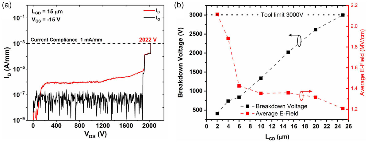
Figure 2: (a) Drain current versus drain bias for 15μm LGD device and (b) breakdown voltage and average electric field plotted against LGD.
The team comments: “Such degradation in average breakdown field with increase in LGD is qualitatively consistent with GaN and Ga2O3 lateral power transistors, contributed by electric field crowding near the drain-side gate edge or gate-side drain edge.”
The researchers compared their work with previous reports of devices demonstrating breakdown voltages exceeding 1kV (Figure 3). Unpassivated devices tend to show higher breakdown parameters than passivated. The Wisconsin-Madison result is only beaten among the passivated devices by its own previous work in the low-breakdown-voltage range.
The researchers point out: “Device passivation plays a critical role in the dynamic performance of lateral HEMTs by suppressing surface traps responsible for current dispersion. Although surface trapping degrades dynamic ON-state behavior, it may beneficially enhance OFF-state robustness by redistributing the electric field at the gate–drain edge, functioning similarly to a field plate and thereby improving breakdown performance.”
The researchers report more than 30% improvement in average breakdown field (more than 1.3MV/cm) at breakdown voltages above 2kV over previously reported state-of-the-art passivated AlGaN HEMTs. The boost is attributed to the use of a gate dielectric, smoothing the electric-field distribution in the gate–drain access/drift region.
The more uniform field increased the BFOM, BV2/RON,sp, to 325MW/cm2 for a 20μm device, based on 2616V BV, and 20.89mΩ-cm RON,sp. The RON was 81.43mΩ-mm.
The researchers also compared their device performances more generally with other devices using ultra-wide-bandgap (UWBG) semiconductor materials (Figure 3).
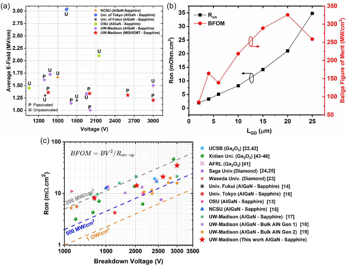
Figure 3: (a) E-field benchmark for lateral AlGaN-channel HEMTs on sapphire substrate, (b) RON and BFOM plotted for various LGD dimensions, and (c) RON versus breakdown voltage benchmarked against state-of-the-art UWBG lateral transistors.
The researchers comment: “When benchmarked against Ga2O3- and diamond-based lateral transistors it demonstrates a performance comparable to that of Ga2O3 and diamond devices while narrowing the gap with state-of-the art Ga2O3 and diamond BFOM values.”
The team looks forward: “Further progress in electric-field engineering, such as systematic field-plate optimization, exploration of alternative device geometries, and improved mesa termination strategies, will be essential to fully realize the potential of this material system.”
MISHEMTs on sapphire AlGaN-channel transistors on sapphire AlGaN
https://doi.org/10.1002/pssr.70190
The author Mike Cooke is a freelance technology journalist who has worked in the semiconductor and advanced technology sectors since 1997.


