


News: LEDs
12 June 2026
Micro-LED transfer via electrochemical etch
University of California Santa Barbara (UCSB) in the USA claims the first demonstration of fully functional vertical micro-scale light-emitting diodes (micro-LEDs), spanning device dimensions down to 3μm, transferred via selective electrochemical etching and direct wafer bonding [Yifan Yao et al, Appl. Phys. Lett., v128, p121103, 2026].
The team comments: “This proof-of-concept demonstration establishes a low-damage, high-throughput pathway for mass transfer of III-nitride devices, enabling scalable heterogeneous integration with various functional platforms for micro-displays, optical communications, and sensing systems.”
Although indium gallium nitride (InGaN) LEDs can be grown on silicon, the performance of such devices tends to be impacted by defects generated by the lattice and thermal mismatch of the respective materials. Silicon platforms are desired for their ability to produce low-cost, large-area electronic drive circuitry, not to mention photonic integrated circuit (PIC) structures, incorporating waveguides and so on.
The alternative method is to transfer reduced defect LEDs produced on more suitable substrates such as bulk or free-standing GaN, or lower-cost sapphire, which is closer to GaN in lattice structural terms than silicon.
A typical method of separation of LEDs from the sapphire growth substrate is laser lift-off (LLO), which involves concentrated laser light thermally decomposing GaN near the substrate, allowing removal and transfer.
The team comments: “Although widely adopted in industry, LLO involves high interfacial temperatures that often exceed the growth temperature of the active region and therefore can induce crystal damage or cracking during the release process and is fundamentally limited to substrates that are transparent to the ultraviolet laser.”
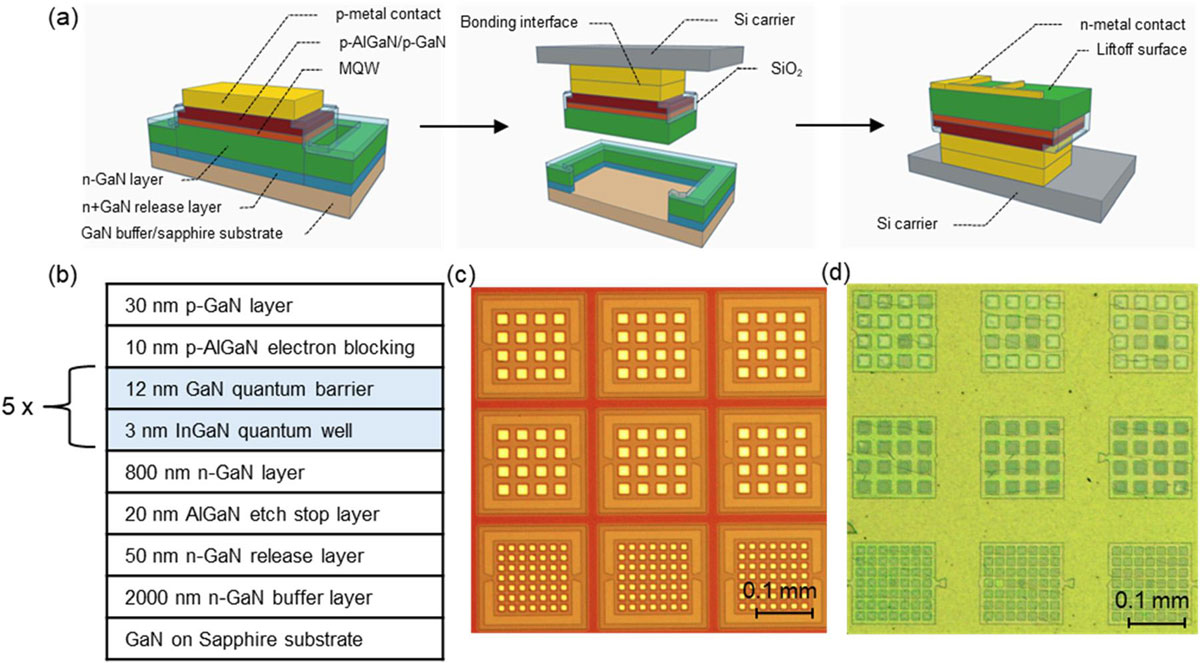
Figure 1. (a) Micro-LED transfer process scheme. (b) Epitaxial structure. Differential interference contrast microscopy false-colored images: (c) before EC etching and bonding (from p-side) and (d) after transfer to silicon carrier substrate (from n-side).
The epitaxial material for the devices included an electrochemical etching release layer of n-type GaN with silicon doping of 1020/cm3, much higher than the other n-GaN layers: less than 3x10¹⁸/cm3 for the 800nm n-GaN device contact layer (Figure 1). An unintentionally doped aluminium gallium nitride (AlGaN) layer served to stop the etching and protect the upper layers.
The researchers comment: “The doping concentration in the release layer is significantly higher than the n-type doping concentration in the rest of the structures, which is essential for the high selectivity of the electrochemical etching process and the structural integrity of the release structure.”
The LED devices were passivated with 25nm atomic-layer-deposited (ALD) silicon dioxide (SiO2). The devices were grouped in uniform 160μm x 160μm pads. Trenches were etched with reactive ions around the pads to expose the etch-release layer sidewalls.
The researchers report: “Employing a uniform pad geometry across different devices minimizes lateral over-etching during the electrochemical etching process and thereby improves uniformity of the release process. Trenches were designed with thin tethers to partially anchor the pad, preventing lateral displacement after the detachment from the substrate.”
The lateral electrochemical etch rate was 20μm/min, much faster than the typical sub-100nm/min of the photoelectrochemical processes often reported. The devices were then flip-chip bonded to a silicon carrier. The bond between the chips and carrier consisted of the p-contact metals of the devices, palladium/aluminium/titanium/gold, and gold contacts on the silicon.
During the thermocompression bonding the pads were vertically lifted-off the growth substrate, breaking the tethers. The researchers explain: “The tethers therefore are designed to be strong enough in the axial direction to ensure spatial registration during electrochemical etching, yet brittle enough to enable rupture during the bonding-induced bending.”
The surface roughness of the electrochemically etched surface was 0.57nm, root-mean-square, according to atomic force microscopy (AFM). A single common n-contact connected the devices in parallel, with single LED addressing available through the separate p-contacts.
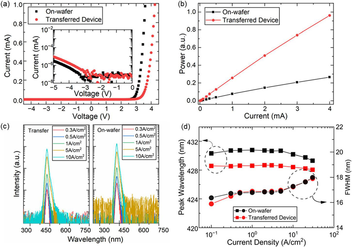
Figure 2. (a) Current–voltage (I–V) characteristics of on-wafer and transferred normal-sized LEDs; inset: log-scaled reverse leakage current. (b) Optical output power. (c) Electroluminescence spectra. (d) Extracted peak wavelength and FWHM as a function of current density.
The diode turn-on voltage of the transferred devices was 3.45V, about 0.5V higher than in measurements on the growth wafer (Figure 2).
The researchers comment: “This can be attributed to the increased contact resistance of the n-type contact (Ti/Au) on the exposed etch-stop layer and increased lateral spreading resistance from thinner n-type GaN layers in transferred devices. Forming a low-resistance contact is inherently challenging on an exposed surface due to the combination of nitrogen polarity and the lack of heavy doping.”
The team suggests a number of strategies to reduce the contact resistance, such as surface pretreatment, different metal contact stacks, and controlled low-temperature post-annealing. The low reverse leakage current after transfer contrasts with laser lift-off processes that suffer from thermal damage and related performance degradation such as increased reverse current, indicating the presence of parasitic current paths.
The output power of the transferred devices demonstrated a 2.2x enhancement over the on-wafer measurements. “This improvement is attributed to the higher light-extraction efficiency of the thin-film flip-chip (TFFC) architecture, in which the released epilayer is bonded onto a reflective Pd/Al/Ti/Au metal contact,” the team explains.
The spectral content of the emissions shows a blue-shift attributed to carrier screening from the quantum-confined Stark effect (QCSE), and full-width at half-maximum (FWHM) broadening from band filling.
The researchers add: “The slight reduction in both peak wavelength and wavelength shift with increasing current observed in the transferred devices is attributed to minor strain relaxation in the active region following the transfer process.”
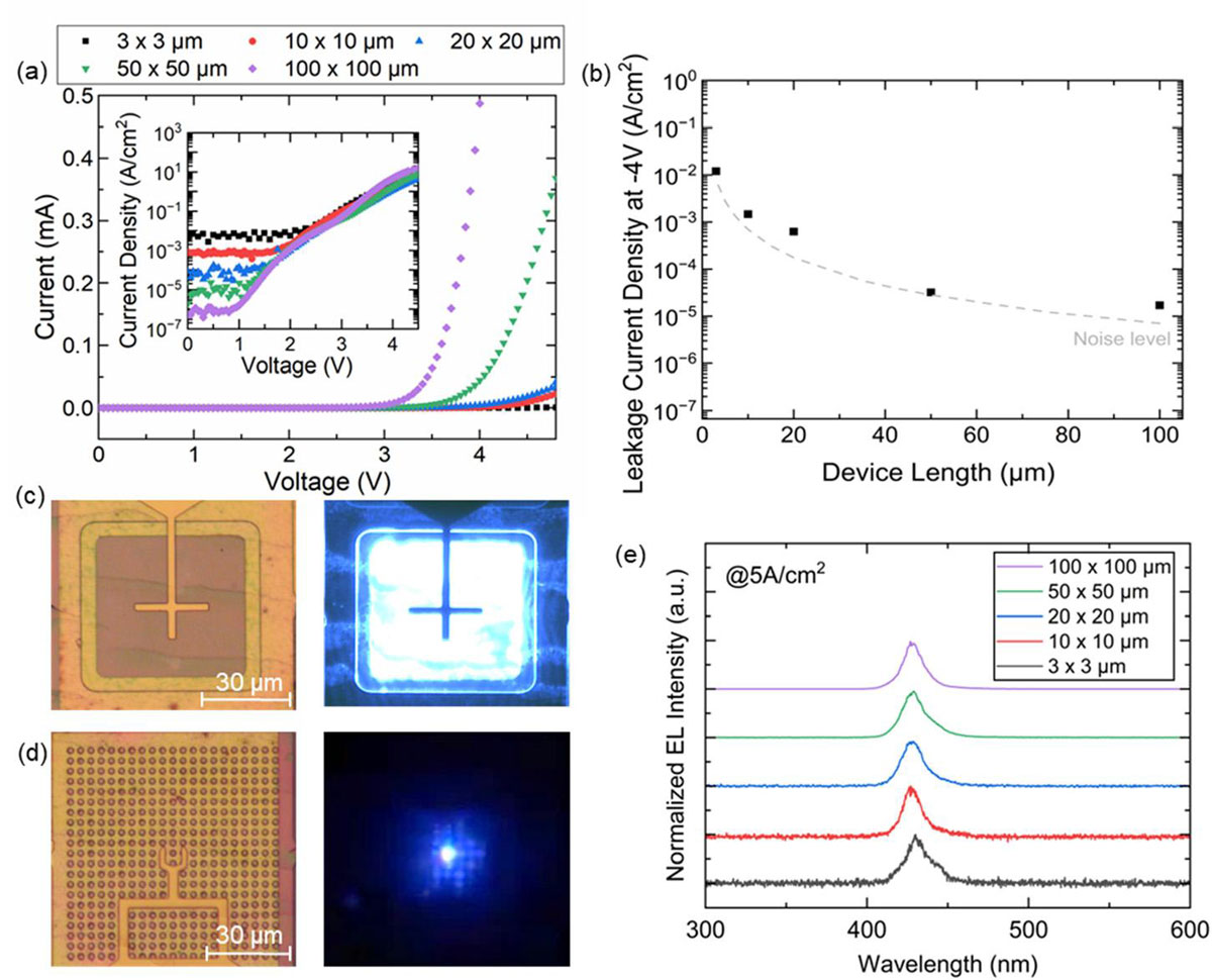
Figure 3. (a) Current density–voltage (J–V) characteristics of transferred micro-LEDs with varied mesa sizes. (b) Reverse leakage current density measured at −4V with instrument noise floor (normalized by mesa area) indicated by dashed line; optical microscope image and emission images of (c) 100μm x 100μm and (d) 3μm x 3μm micro-LED arrays. (e) Normalized electroluminescence spectra at 5A/cm2.
The square device sizes were varied between side lengths of 100μm down to 3μm (Figure 3). These were arranged in arrays, where allowed by the 160μm pad size.
The researchers report: “The leakage current density measured at −4V exhibits clear size dependence and remains low for all device sizes, comparable to state-of-the-art InGaN micro-LEDs.”
As the exposed length of the dry-etched side walls of the smaller devices increases, so does the opportunity for parasitic current leakage paths to form there.
https://doi.org/10.1063/5.0327220
The author Mike Cooke is a freelance technology journalist who has worked in the semiconductor and advanced technology sectors since 1997.


