


News: Microelectronics
22 June 2026
Monolithic bidirectional diamond switch
Researchers in Japan claim the first fabrication of monolithic bidirectional diamond switches based on two-dimensional hole gas (2DHG) structures [Sora Kawai et al, Appl. Phys. Express, v19, p041002, 2026].
The on-resistance (Ron) was reduced by more than an order of magnitude, down to 8.2mΩ-cm2 relative to bidirectional switches using a deep-depletion structure in diamond. The blocking capability was maintained up to 290V, also an improvement on deep-depletion diamond switches that suffer from high current leakage in the blocking state.
The researchers from Power Diamond Systems Inc, Waseda University, and Kyushu Institute of Technology, see potential deployment in single-stage on-board chargers for electric vehicles. Single-stage charger circuit topologies based on bidirectional switches reduce costs and increase power density over two-stage systems.
The researchers comment: “There are two main types of bidirectional switches: the dual field-effect transistors (FETs) type, in which two FETs are connected back-to-back, and the monolithic type, in which two gates are integrated on a single FET structure. In terms of on-resistance, footprint and cost, monolithic bidirectional switches are the preferred solution.”
Diamond offers a wide 5.47eV bandgap, along with high carrier mobilities: 2000–3800cm2/V-s for holes and 4500cm2/V-s for electrons. The wide bandgap also means that the critical electric field can reach 10MV/cm before breakdown.
In addition, diamond has a high thermal conductivity of 22W/cm-K, which would be beneficial for high-heat-dissipation power devices.
A 2DHG channel can be created using hydrogen plasma surface treatment. By contrast, the deep-depletion method of boron doping to achieve a bulk conduction channel suffers due to the large 0.37eV (370meV) activation energy of the acceptor state. Since room temperature is equivalent to about 26meV, the carrier density is low, increasing on-resistance. Subjecting deep-depletion devices to high temperature can therefore reduce on-resistance significantly.
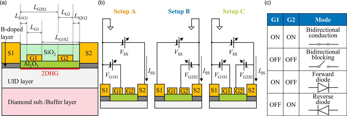
Figure 1: (a) Monolithic diamond bidirectional switch. (b) Evaluation setups: A and B for transfer, output and breakdown characteristics, and C for specific bidirectional switch operations. (c) Operation modes.
The switches (Figure 1) were fabricated by using epitaxial material from microwave plasma chemical vapor deposition (MPCVD) on diamond substrate. Two layers were deposited: 500nm diamond buffer, and 200nm unintentionally doped (UID) diamond.
Further (selective area) MPCVD created the two source contact regions, doped with boron (B). Hydrogen plasma treatment formed the 2DHG by hydrogen termination. Oxygen plasma isolated the devices. During the oxygen plasma exposure the device regions were protected by patterned photoresist.
The gate stack consisted of 200nm aluminium oxide (Al2O3) insulator, and 200nm aluminium metal. The insulator was deposited by atomic layer deposition at 450°C. The oxidant was water vapor (H2O).
Plasma-enhanced chemical vapor deposition (PECVD) silicon dioxide (SiO2) provided further insulation through which the sputtered titanium/aluminium source electrodes were deposited and patterned.
The main device reported on had 50μm gate width. The distance between the gates and nearest source contacts was 1μm (i.e. LS1G1, LS2G2). The gate lengths were 2μm (LG1, LG2). The cross-distance between the gates and furthest sources was 8μm (LS1G2, LS2G1).
With the supply voltage (VSS) at ±10V, for setups A, B, the on/off current ratio was more than 8 orders of magnitude. The setup A, +10V VSS, had a Vth threshold of 35.5V. The threshold for B, −10V, was 36.6V. The maximum output currents were −249mA/mm and +243mA/mm for A and B, respectively.
The breakdown voltage (100nA/mm) for setup A was −290V; for B it was +310V. The average electric field (290V/8μm) was of order 0.36MV/cm. Waseda has previously reported 2DHG diamond transistors where the breakdown electric field reached 1MV/cm.
The researchers attribute the poorer breakdown performance of the bidirectional switch to the electric field near the gate electrode. They believe that an optimized electric field distribution could enhance the breakdown performance.
The team offers some suggestions: “For example, incorporating a field-plate structure would be an effective approach to mitigate the electric field near the gate electrode, thereby increasing breakdown voltage. By reducing the electric field, the gate insulator can be made thinner; therefore, a field-plate structure is expected to also contribute to a reduction in the Vth.”
In bidirectional conduction mode, with −20V gate potentials, the on-resistance was estimated at 74.2Ω-mm (Figure 2). In blocking mode, +55V gate, the current remained less than 10nA/mm with the supply in the range −100V to +100V.
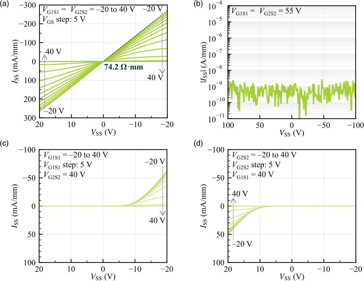
Figure 2: (a) Bidirectional conduction, (b) bidirectional blocking, (c) forward diode conduction, and (d) reverse diode conduction, of bidirectional switch under setup C.
The researchers comment: “The observation of the four operation modes unique to bidirectional switches indicates that the monolithic bidirectional 2DHG diamond switches have been successfully realized.”
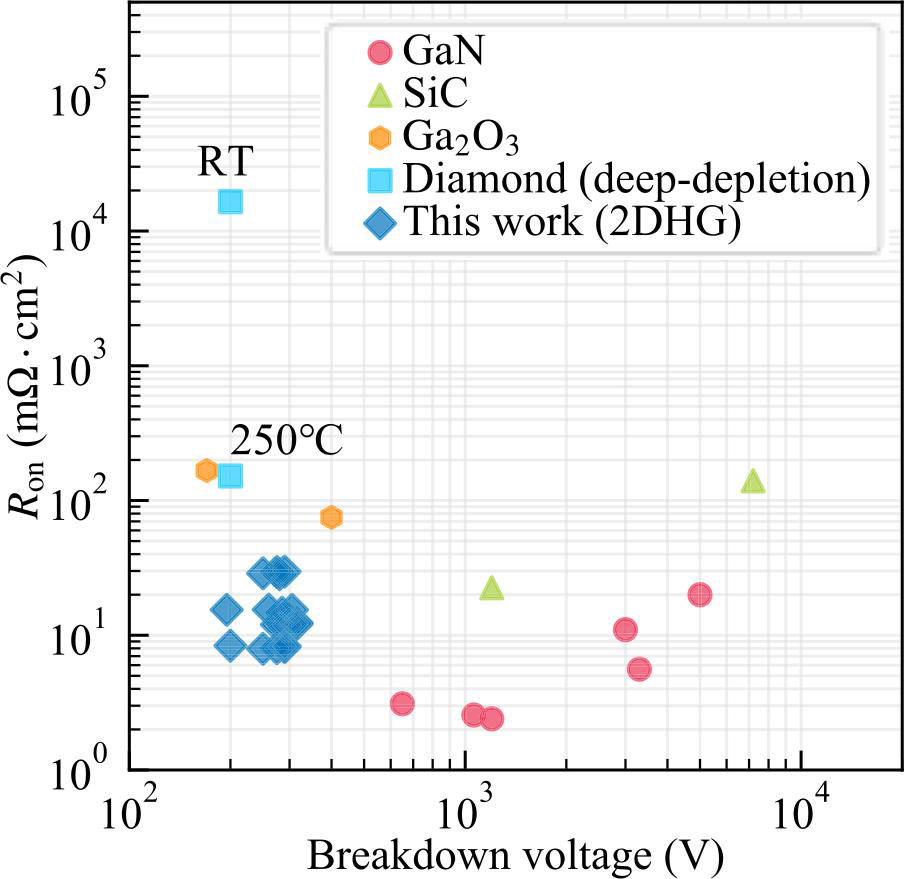
Figure 3: Bidirectional switch benchmarks of breakdown voltage versus on-resistance. Temperature information is for deep-depletion-type diamond switch. Devices reported by team include three other variations of gate lengths and gate-source distances.
The researchers present a comparison of their devices against bidirectional switches in various semiconductor materials (Figure 3). While the on-resistance is competitive with gallium nitride (GaN) and silicon carbide (SiC) devices, the breakdown voltage of the diamond devices clearly needs work.
Monolithic bidirectional diamond switch FETs GaN SiC MPCVD
https://doi.org/10.35848/1882-0786/ae5bdd
The author Mike Cooke is a freelance technology journalist who has worked in the semiconductor and advanced technology sectors since 1997.


