


News: LEDs
22 June 2026
Tunnel-junction micro-LEDs with 45% wall-plug efficiency
Researchers in China report on tunnel-junction (TJ) blue micro light-emitting diodes (LEDs) reaching wall-plug efficiencies of 45.23% [Yao Wang et al, Optics Express, v34, p17683, 2026]. The researchers used a device structure that avoided the post-growth thermal annealing, which is normally applied to activate the magnesium doping needed to realize p-type gallium nitride (p-GaN).
“This work eliminates the risks of thermal-induced epitaxial degradation and paves the way for applications of annealing-free tunnel-junction micro-LEDs in vertically stacked full-color micro-LED displays, high-brightness lighting applications, and other optoelectronic devices,” comments the team from Xiamen University, Future Display Institute of Xiamen, and Nanjing University.
Particularly prone to damage are the indium gallium nitride (InGaN) multiple quantum wells (MQWs) that are used to emit blue photons under electrical bias.
Micro-LEDs are being actively developed for use as pixels in the ultra-high-definition displays deployed in virtual/augmented reality (VR/AR) and other systems. Advantages of compound semiconductor LED pixels include higher resolution, lower power consumption, longer lifespan, increased brightness, and faster response time.
GaN-based LEDs often suffer from difficulties on the hole injection side. Thermal annealing is typically used to drive out hydrogen that passivates the acceptor states provided by Mg. The resulting p-GaN tends to have low conductivity. TJ structures with n-GaN top layers could solve some of the problems, but activation of the buried p-GaN becomes tricky.
The researchers used a top n-GaN layer grown at low temperature to encourage island-like growth. This created gaps in the surface, enabling escape of hydrogen from the underlying p-GaN.
The researchers used metal-organic chemical vapor deposition on patterned sapphire substrates to grow the blue LED material. Apart from the tunnel junction (TJ), the process was standard. The growth sequence for the TJ was 20nm 1000°C heavily doped p+-GaN, a 3nm 680°C n-InGaN layer, and 20nm 720°C n+-GaN. The growth surface was treated between each step with cleaning solvent and aqua regia.
A final lightly doped 300nm n--GaN layer was grown at “low temperature”, 865°C, to promote island growth. This “island-structured TJ micro-LED (Isl TJ)” was compared with a reference device that had a smooth top n--GaN layer grown at a more conventional 950°C.
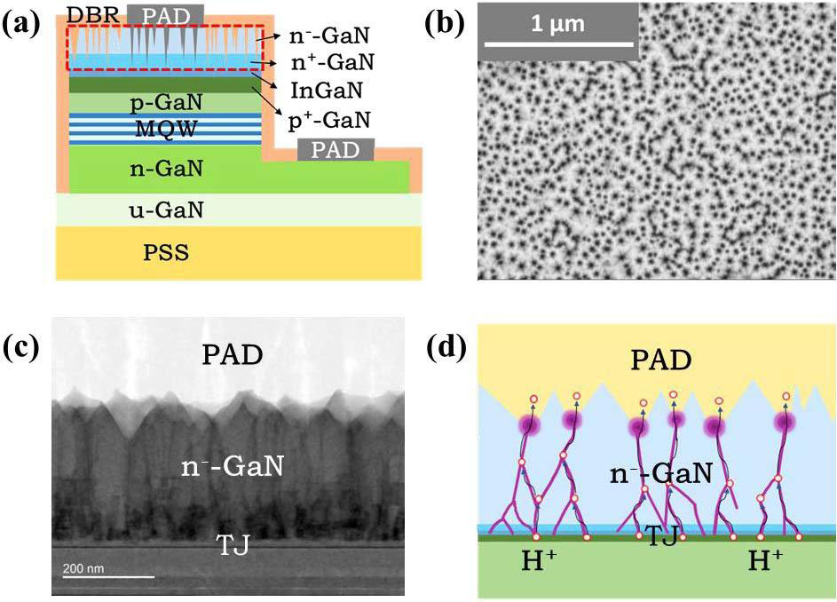
The III–N materials were fabricated into 10μm LEDs with inductively coupled plasma etched mesas (Figure 1). The sidewalls were passivated by a “lightweight atomic charge-matching passivation technique”, previously developed by the team. This involves wet etching and hydrogen plasma treatments. A further 230nm of plasma-enhanced chemical vapor deposition silicon dioxide was used for electrical insulation.
Light extraction was enhanced with distributed Bragg reflectors consisting of titanium- and silicon-dioxide layers. The metal contacts were chromium/titanium/gold. Some devices were subjected to 30-minute 720°C rapid thermal annealing (RTA) after the mesa etching step.
Apart from enabling the passivating hydrogen to escape from the p-GaN layers, the researchers also suggest that the subsequent metal contact layer forms nanoscale sharp tips in the n--GaN: “Under electrical bias, these metallic tips induce local field enhancement, and the concentrated electric field propagates along the dislocation lines, further enhancing carrier injection and contributing to the superior optoelectronic performance of Isl TJ.”
The researchers found that the Isl TJ micro-LEDs without RTA produced nearly double the spectral electroluminescence intensity over all the other fabricated devices. The team comments: “This significant improvement suggests superior carrier injection and radiative recombination efficiency within the Isl TJ structure.”
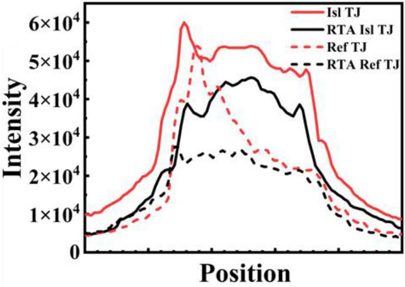
Figure 2: Line-scan intensity profiles.
The intensity profile of the Isl TJ device was also more uniform than the reference without RTA (Figure 2). The researchers attribute this to better current spreading and more complete activation of the underlying p-GaN in the Isl TJ. The team also notes that the impact of RTA is different: for the reference, RTA improves uniformity at the cost of luminescence, “possibly due to induced damage in the MQWs”; conversely, RTA of the Isl TJ “results in a degradation of both optical performance and uniformity,” according to the team. The researchers suggest that Isl TJ with RTA suffer damage detrimental to the MQWs.
In terms of the peak position and width, all devices suffered a 14–15nm blue-shift in wavelength, along with a full-width at half-maximum broadening of 12–13nm, as the injection current density increased to 350A/cm2.
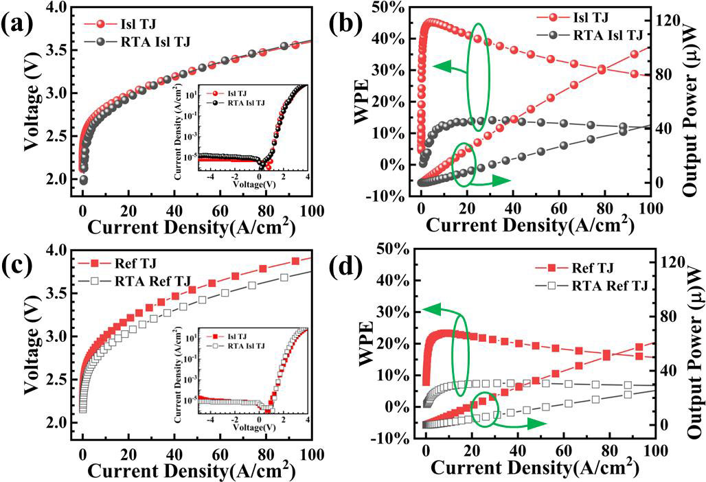
Figure 3: (a) Current–voltage characteristics and (b) wall-plug efficiency (WPE) and output power curves for Isl TJ devices. (c) and (d) reference comparisons. Insets in (a) and (c) show corresponding reverse leakage current curves.
The Isl TJ micro-LED without RTA achieved a low voltage of 2.99V and 2.55μW output power at 20A/cm2 injection, and up to 45.23% WPE (Figure 3).
“This indicates that the p-GaN in the Isl TJ has been sufficiently activated during epitaxial growth, resulting in efficient tunnel junction that minimizes voltage drop and enhances carrier injection,” the researchers comment.
RTA adversely affected the output power (18.21μW) and peak WPE (14.12%). The team explains: “This severe degradation confirms that the RTA process damages the MQWs in this structure, overriding any potential electrical benefit.”
The researchers also see the rough surface of the Isl TJ as offering optical enhancement through suppression of total internal reflection, which occurs with smooth-surface III-N devices. This reflection traps light within the device structure.
The team notes that the 45.23% WPE for the Isl TJ without RTA beats that of other blue LEDs reported with TJ (3.4%) and indium tin oxide (up to 34.3%) current spreading/hole injection structures.
Tunnel-junction micro-LEDs InGaN
https://doi.org/10.1364/OE.592151
The author Mike Cooke is a freelance technology journalist who has worked in the semiconductor and advanced technology sectors since 1997.


