

News: Suppliers
9 July 2026
Sandia selects LayTec’s EpiX mapping station for optical wafer characterization
Optical in-situ metrology system maker LayTec AG of Berlin, Germany says that Sandia National Laboratories has purchased a customized manual-loading version of its EpiX mapping station, combining white light reflectance (WLR) and photoluminescence (PL) metrology for non-contact optical wafer mapping.
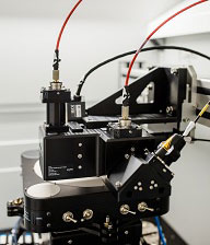 Picture: EpiX XYZ mapping stage and WLR + PL optics.
The system comes in a UV–vis configuration optimized for aluminium gallium nitride (AlGaN) power, RF, and optoelectronic applications, as well as novel materials, supporting Sandia’s advanced semiconductor research by providing spatially resolved insight into key wafer properties. EpiX is said to uniquely enable 2D mapping of parameters such as layer thickness, composition-related optical signatures and luminescence characteristics for high-electronic-mobility transistors (HEMTs) and other device structures, helping researchers to evaluate uniformity across complex semiconductor wafers.
“The customized configuration reflects exactly what EpiX was designed for: flexible, high-quality optical wafer characterization for demanding compound semiconductor R&D,” says LayTec’s CEO Volker Blank.
LayTec launches EpiX modular wafer mapping station for compound semiconductor R&D