


News: Suppliers
13 January 2026
Wolfspeed produces single-crystal 300mm silicon carbide wafer
Wolfspeed Inc of Durham, NC, USA — which makes silicon carbide (SiC) materials and power semiconductor devices — has announced what it says is a significant industry milestone with the production of a single-crystal 300mm (12-inch) silicon carbide wafer. Backed by a silicon carbide IP portfolios comprising more than 2300 issued and pending patents worldwide, Wolfspeed is pioneering the transition to 300mm technology, establishing a path to future volume commercialization.
The technology advance is targeted at next-generation computing platforms, immersive augmented reality/virtual reality (AR/VR) systems, and high-efficiency, advanced power devices. By expanding silicon carbide to 300mm, Wolfspeed says it is boosting performance thresholds and manufacturing scalability for demanding semiconductor applications.
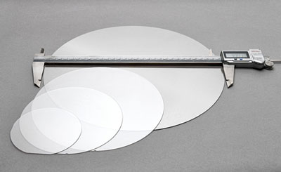 Picture: Wolfspeed’s silicon carbide wafers, scaling up to 300mm.
“Producing a 300mm single-crystal silicon carbide wafer is a significant technology achievement and the result of years of focused innovation in crystal growth, boule and wafer processing,” says chief technology officer Elif Balkas. “It positions Wolfspeed to support the industry’s most transformative technologies, especially critical elements of the AI ecosystem, immersive augmented and virtual reality systems, and other advanced power device applications.”
Wolfspeed’s 300mm platform will unify high-volume silicon carbide manufacturing for power electronics with advanced capabilities in high-purity semi-insulating substrates used in optical and RF systems. Such convergence can support a new class of wafer-scale integration across optical, photonic, thermal and power domains, the firm adds.
AI – unlocking More than Moore
As AI workloads push data centers to their power limits, the demand for improved power density, thermal performance, and energy efficiency will continue to accelerate, expects Wolfspeed. The firm reckons that its 300mm silicon carbide technology will enable the integration of high-voltage power delivery systems, advanced thermal solutions, and active interconnects at wafer scale, extending system performance beyond traditional transistor scaling.
AR/VR – powering optical and thermal integration
Next-generation AR/VR systems require compact, lightweight configurations that integrate high-brightness displays with expansive fields of view and effective thermal management. Silicon carbide’s unique material properties, including mechanical strength, thermal conductivity, and optical refractive control, make it ideal for multi-functional optical architectures, reckons Wolfspeed.
Beyond AI infrastructure and AR/VR, transitioning silicon carbide to a 300mm platform represents a major step forward in scaling the production of advanced power devices, the firm adds. The larger wafer diameter enhances the ability to cost-effectively meet growing demand for applications including high-voltage grid transmission and next-generation industrial systems.
“This 300mm breakthrough is more than a technical milestone — it unlocks new opportunities for silicon carbide as a strategic material,” comments Poshun Chiu, principal analyst, Compound Semiconductor, at market analyst firm Yole Group. “It clearly demonstrates that silicon carbide is advancing to the next level of manufacturing maturity required for the coming decade of electrification, digitalization, and AI,” he adds. “It provides the market with a credible roadmap toward higher-volume production, improved economics and long-term supply assurance [see the report ‘Power SiC 2025 – Front-End Manufacturing Equipment’ and ‘Power SiC 2025 – Markets and Applications’].”
Wolfspeed cuts quarterly loss after CapEx slashed during restructuring
Wolfspeed announces commercial launch of 200mm silicon carbide wafers


