


News: Microelectronics
26 January 2026
Increasing 2DEG density with aluminium nitride barriers
University of Michigan at Ann Arbor in the USA has reported the experimental demonstration of a record room-temperature 2DEG sheet density exceeding 1x1014cm2 in a single-channel AlN/GaN heterostructure grown by plasma-assisted molecular beam epitaxy (PAMBE), using a 9nm-thick AlN barrier [Shubham Mondal et al, Appl. Phys. Lett., v127, p243505, 2025].
The researchers see their work as potentially leading to high-performance, thermally robust, and aggressively scaled devices for millimeter-wave power amplifiers, RF front-end modules, and wide-bandgap electronic applications. The team adds: “For practical device implementations, dielectric integration (e.g. Al2O3 or HfO2) and optimized interface engineering provide a more robust and reliable design window for AlN/GaN HEMTs.”
Typical lateral HEMT structures engineer a two dimensional electron gas (2DEG) channel by growing undoped GaN and adding a barrier layer, usually aluminium gallium nitride (AlGaN). Alternative barriers such as indium- (InAlN) or scandium- (ScAlN) AlN alloys offer higher mobility but at the expense of much lower 2DEG carrier density.
The researchers comment: “In contrast, AlN/GaN exhibits the largest spontaneous and piezoelectric polarization difference among III-nitrides, supporting record-high 2DEG density and strong confinement when strain is well managed.”
Strain and spontaneous charge-related polarization differences between the channel and barrier layers creates a potential well for the electrons near the barrier/channel layer interface.
The researchers used a high-resistivity GaN-on-sapphire template on which 100nm GaN was re-grown along with a variable-thickness AlN barrier. The GaN template layer was vanadium-doped to achieve high resistivity.
The heterostructure was capped with GaN to protect the AlN from degradation processes in the atmosphere, such as oxidation to which Al-containing material is particularly prone.
The growth method was 600°C PAMBE under metal-rich conditions for improved coalescence and surface planarization. The team explains: “The excess metal enhances adatom mobility, fostering lateral growth and smoother film surfaces.”
The researchers used van der Pauw Hall-effect measurements to extract the 2DEG carrier density, mobility and sheet resistance (Figure 1). For all the samples the trend in mobility was downwards from 925.2cm2/V-s as the barrier thickness increased from 3nm.
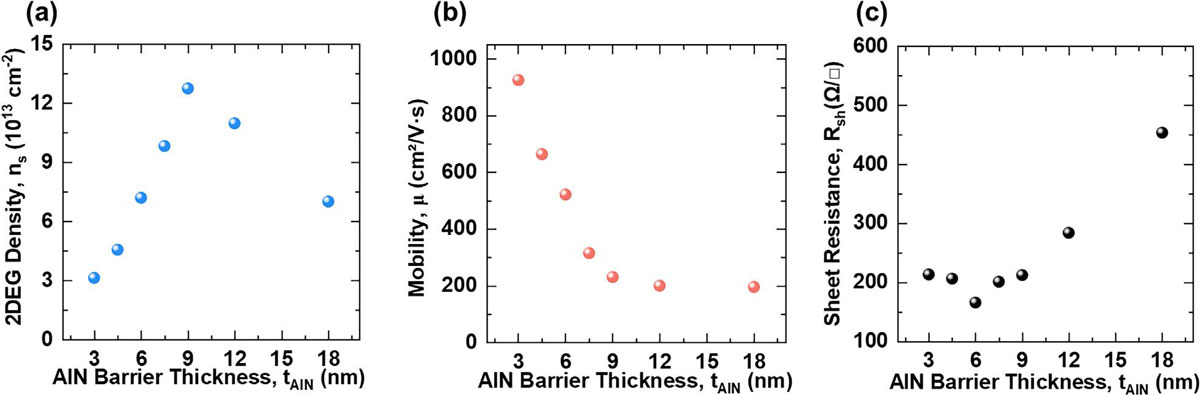
Figure 1: Plots of room-temperature van der Pauw Hall measurements: (a) 2DEG density (ns), (b) mobility (μ), and (c) sheet resistance (Rsh) versus AlN barrier thickness (tAlN).
The maximum 2DEG density was obtained in the 9nm-barrier sample: 1.3x1014cm2. The researchers comment: “This record value arises from optimized MBE growth featuring precise strain control and an atomically sharp GaN/AlN interface.”
The lowest sheet resistance, combining the density and mobility trends, was 166Ω/□, obtained for the 6nm-barrier sample, “comparable to the uppermost-performing values reported for AlN/GaN heterostructures,” according to the team. The sheet resistance is inversely proportional to the mobility and 2DEG carrier density.
One factor impacting sheet resistance in the 9nm-barrier sample was the appearance of cracks, indicating partial strain relaxation. The 6nm sample achieved a 7.8x1013cm2 2DEG density.
The team comments: “The formation of cracks can be minimized by further optimizing growth parameters and/or through strain engineering such as selective-area epitaxy, such that the exceptionally high 2DEG density can be fully exploited in next-generation HEMTs, such as Fin-HEMTs as well as multi-channel devices.”
Theoretical considerations suggest the critical thickness for strain relaxation to occur for AlN on GaN is around 6.5nm. The researchers add: “It should be noted that surface-roughness-induced dislocations can develop at thicknesses well below the theoretically predicted critical values, contributing to the wide range of critical thicknesses reported in the literature. However, by carefully tuning our epitaxial growth conditions, we were able to preserve the structural integrity of the AlN barrier even beyond the critical thickness. This enables the formation of a record-high 2DEG density at the AlN/GaN interface.”
Three main scattering components are used to explain mobility reduction: collisions between the carriers through the Coulomb force, carrier-polar optical phonon collisions, and carrier collisions with rough interfaces (not helped by cracks). The surface roughness from 2μmx2μm area atomic force microscopy (AFM) was 0.28nm for 9nm barriers, and 0.21nm for 6nm. The surface roughness is presumably reflective of interface roughness.
I note that there appears to be a downwards kink between the 6nm and 7.5nm mobility measurements, suggesting the enhancement of a collision mechanism, such as interface scattering. The downward mobility trend between the thinnest 3nm barrier and 9nm is explained by the increased carrier density increasing the Coulomb scattering rate. The researchers comment: “Increasing the AlN barrier thickness beyond 6nm results in partial relaxation and 2DEG localization near relaxation-induced defects, causing enhanced carrier scattering and elevated Rsh.”
The researchers also studied the Hall effect at low temperature (Figure 2). The sheet resistance at 300K was 175Ω/■. The extracted parameters show almost constant performance up to around 100K, when temperature-dependent factors come into play. The finite 2DEG density at low temperature suggests that carrier freeze-out does not occur, indicating that “2DEG in AlN/GaN is polarization-induced rather than donor-supplied, and contributions from buffer conduction or unintentional silicon incorporation are negligible”.
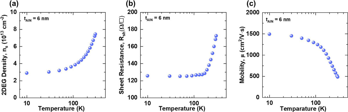
Figure 2: Temperature-dependent Hall-effect measurements for 6nm AlN barrier sample: (a) ns, (b) μ, and (c) Rsh for range 10–300K.
The increased carrier density at higher temperatures is attributed to “lattice contraction and corresponding modifications in piezoelectric polarization, PPZ, and band alignment”
The researchers comment: “These observations highlight the robustness of carrier transport and confirm the suitability of the device for reliable operation in cryogenic electronic and quantum applications.”
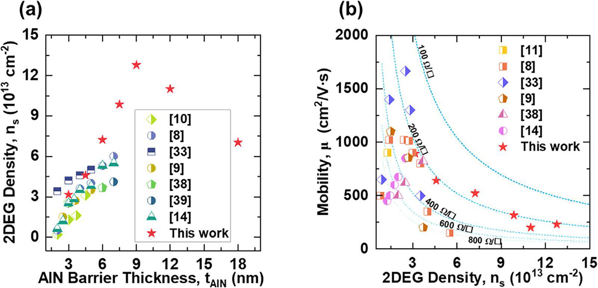
Figure 3: Benchmarks against previous reports: (a) 2DEG density versus AlN barrier thickness; (b) sheet resistance versus 2DEG density.
The researchers also report benchmark comparisons with previous reports of AlN barrier/GaN heterostructures (Figure 3). The team comments: “These findings clearly demonstrate that it is possible to realize exceptionally high 2DEG densities without compromising sheet resistances in AlN/GaN heterostructures.”
Aluminium nitride barriers GaN AlN/GaN heterostructure HEMT AlGaN
https://doi.org/10.1063/5.0294027
The author Mike Cooke is a freelance technology journalist who has worked in the semiconductor and advanced technology sectors since 1997.


