


News: Optoelectronics
8 January 2026
Marktech launches new transfer-molded LED and photodiode packaging capabilities
Marktech Optoelectronics Inc of Latham, NY, USA and its device manufacturing partner Optrans Corp of Kawasaki-Shi, Japan are introducing new transfer-molded photodiode and LED packaging capabilities, which are currently under development and scheduled for first customer availability in second-quarter 2026. The next-generation photonics packages offer improved reliability, optical beam control, enhanced environmental robustness, and reduced stray-light interference while supporting both conventional LED emitters and advanced point-source resonant-cavity light-emitting diode (RCLED) and quantum well light-emitting diode (QWLED) architectures.
Transfer molding forms a precision optical and mechanical structure directly over the die, encapsulating the LED or detector in a controlled molding process that produces what is claimed to be exceptional part-to-part uniformity, tighter beam profiles, stronger wire-bond protection, and improved long-term reliability under temperature and humidity stress. This approach offers significant advantages over traditional packaging methods — such as glob-top epoxy, liquid potting, COB silicone domes, and discrete lens cap assemblies — making it especially well suited to industrial, medical, instrumentation, aerospace and automotive applications that require repeatable performance, a small footprint for dense packing, and robust handling.
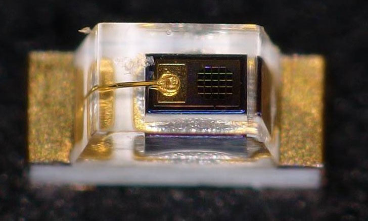
Picture: Prototype transfer molded package (under development).
“Transfer molding gives us exceptional control over optical geometry, reliability, and manufacturing scalability,” says Optrans’ chief technical officer Vince Forte. “This is especially important for point-source LEDs where beam shape and emitter alignment directly impact system performance.”
Improved optical performance
Transfer-molded packages allow for integrated primary optics, enabling tightly controlled lens profiles for beam shaping, collimation, and fiber- or aperture-coupling. This is particularly valuable for RCLED and QWLED point-source emitters, where sub-millimeter optical alignment is required for measurement, medical, aiming and sensing applications. The molding process also provides what is claimed to be excellent control over emitter-to-lens alignment, ensuring that the optical axis is precisely maintained from unit to unit — critical for applications requiring tight beam symmetry or long-distance projection. Transfer-molded materials can be engineered for high UV, visible or IR transmission, enabling improved radiant flux output and enhanced optical efficiency. In addition, the package structure reduces internal reflections and minimizes angular variation, resulting in more uniform and predictable emission profiles. Furthermore, phosphor additives can be incorporated directly into the molding compound to convert or broaden the LED’s native emission spectrum, enabling tailored spectral outputs — such as multi-band, white-light, or application-specific wavelengths — without the need for external filters or secondary optics.
Detection performance can also be optimized using a transfer-molded photodiode package. For instance, transfer-molded packages allow for integrated primary optics, enabling tightly controlled lens profiles for beam shaping, collimation and coupling. In addition, the transfer-molded photodiode package minimizes stray light, reduces parasitic reflections, and maintains tighter alignment tolerances, resulting in higher signal-to-noise ratio and more accurate detection. It also provides consistent optical geometry and mechanical stability, ensuring repeatable responsivity and improved low-light performance. Transfer-molded packaging can reduce parasitic capacitance because epoxy molding compounds typically have a lower dielectric constant (εr ≈ 3.5–4.5) compared to ceramic, glass-to-metal seals, or large metal package volumes. By reducing parasitic capacitance and enhancing thermal dissipation, transfer-molded photodiode packages further enable faster response times and greater precision in demanding sensing applications — all within a compact, reliable, production-scalable form factor. Furthermore, when the molding compound is formulated with optical filtering characteristics, it can function as an integrated bandpass or notch filter, selectively transmitting or blocking specific wavelengths to enhance detection accuracy in targeted spectral bands.
Better reliability and environmental robustness
Mechanical stability is also enhanced, as the molded compound encapsulates and protects the LED die, improving vibration resistance and long-term reliability in harsh environments. Wire bonds in conventional, non-encapsulated packages can fail by lift-off (wire debonding) or wire fracture due to mechanical stress from vibration, impacts, and thermal cycling. A monolithic molded package structure protects the die and wire bonds from shock, vibration, thermomechanical fatigue, and water ingress, resulting in enhanced durability and more consistent performance across temperature and mechanical extremes. This makes optoelectronic transfer-molded packaging technology a suitable choice for automotive, industrial, aircraft and defense-grade requirements.
Low-profile, compact footprint, and dense packing
Transfer-molded SMD optoelectronic packages offer a significantly smaller footprint than many conventional SMD LED and photodiode package styles because the optical and mechanical structures — such as lenses, light shields, and housings — are formed directly in the molded body rather than added as separate plastic components. By eliminating bulky reflector cups, multi-part lens caps, and oversized lead frames, transfer-molded packages can achieve tight lateral dimensions and low profiles, often in standard JEDEC outlines optimized for automated pick-and-place.
This reduced footprint enables much denser component packing on printed circuit boards (PCBs), supporting higher channel counts in sensing arrays, more compact illumination modules, and miniaturized instrumentation. As electronics continue to shrink in size and increase in functional complexity, the compactness of transfer-molded SMD optoelectronics provides a critical advantage — allowing designers to integrate more optical functionality into smaller form factors without sacrificing performance or reliability.
Manufacturing consistency and cost efficiency
Compared to liquid or manually formed encapsulants, transfer molding provides repeatable geometry, minimal unit-to-unit variation, and scalability for high-volume production. Once tooling is in place, the process yields lower per-unit cost with tight control over height, planarity, lens radius, and package outline.
Availability
Engineering prototypes are planned for release in early 2026, with full production availability beginning in Q2/2026. Transfer-molded photodetector and LED packages will be available in select JEDEC and IPC SMD footprints. Custom sizes and optical geometries can be developed to OEM design specifications. Additional potential photonics packaging variations include options for integrated lenses, phosphor layers, filter windows, and light shielding. Initially, chip sizes up to 350µm x 350µm can be packaged. The new transfer-molded packaging is suitable for emission and detection of wavelengths from 355nm to 2300nm.
Engineering samples and custom design engagements are welcome upon request.
Marktech Optoelectronics is exhibiting in booth #259 at SPIE Photonics West 2026 in San Francisco, CA, USA (17–22 January).
Optrans and Marktech add UVA (365nm, 395nm) and near-UV (405nm) to UV LED range


