


News: Optoelectronics
20 January 2026
CEA-Leti advances silicon-integrated quantum cascade lasers for mid-IR photonics
At SPIE Photonics West 2026 in The Moscone Center, San Francisco, CA, USA (20–22 January), micro/nanotechnology R&D center CEA-Leti of Grenoble, France is presenting new research highlighting major progress in the integration of quantum cascade lasers (QCLs) with silicon photonic platforms for mid-infrared (MIR) applications.
The paper ‘Advanced Architectures for Hybrid III-V/Silicon Quantum Cascade Lasers: Toward Integrated Mid-Infrared Photonic Platforms’ compares three complementary hybrid laser architectures that collectively advance the practicality, flexibility and scalability of MIR photonics.
Toward ‘Smaller, More Robust, and More Manufacturable MIR Systems’
Mid-infrared light plays a critical role in technologies such as gas sensing, chemical spectr oscopy, biomedical diagnostics, and security, because many molecules exhibit strong absorption signatures in this spectral region. Despite the technology’s importance, MIR photonic systems remain large, costly and difficult to manufacture at scale. Integrating MIR light sources directly onto silicon photonic platforms offers a path toward smaller, more robust and more manufacturable systems — bringing mid-infrared photonics closer to the level of integration in the near-infrared.
Three architectures, three integration strategies
In its Photonics West presentation, CEA-Leti demonstrated and compared three distinct hybrid III-V/silicon QCL architectures, each addressing a different integration challenge:
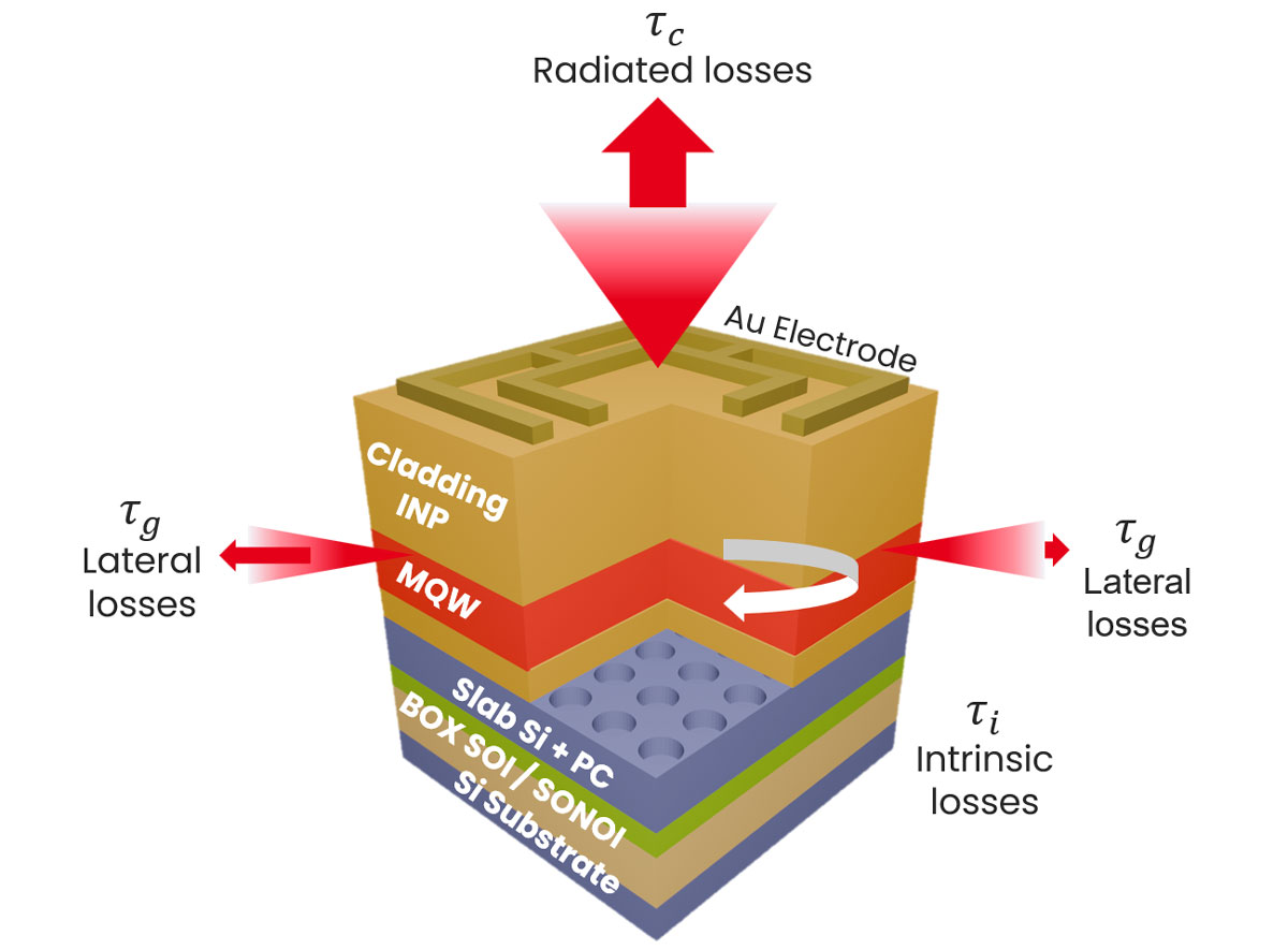
- Hybrid Distributed Feedback QCL on Silicon-on-Nothing-on-Insulator with Adiabatic Coupling
This approach enables robust single-mode emission around 4.3µm with efficient optical power transfer from the III-V active region into silicon waveguides. High-index-contrast silicon photonics provide precise feedback and light routing, making this architecture well suited for scalable photonic integrated circuits targeting spectroscopy and chemical sensing. - Hybrid QCL with an External Silicon Distributed Bragg Reflector Cavity
In this configuration, optical gain and optical feedback are decoupled: the III-V material provides amplification, while wavelength selection and feedback are implemented in silicon using distributed Bragg reflector (DBR) cavities. This separation offers enhanced design flexibility and opens a clear path toward tunable and multi-functional MIR sources for advanced spectroscopic and sensing systems. - Ultra-Compact QCL Micro-Sources Based on Photonic Crystals & Micro-Rings
Miniature light sources in these devices achieve footprints below 100µm2 by leveraging strong optical confinement and resonant effects. The resulting extreme miniaturization enables dense on-chip integration and supports new system architectures where size, power consumption, and integration density are critical.
Picture: III-V/Si photonic crystal surface-emitting QCL & micro-resonator ring. Credit: Alexis Holb.
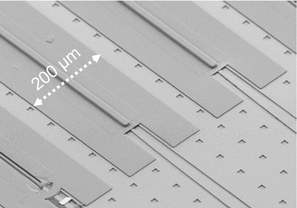
Picture: III-V/Si distributed feedback QCL. Credit: Maxime Lepage.
From passive platform to active host
Collectively, the results show that silicon photonics can play an active role in mid-infrared laser systems. By combining adiabatic optical coupling, silicon-based feedback and cavity engineering, and ultra-compact laser concepts, CEA-Leti establishes several viable integration pathways rather than a single one-size-fits-all solution. The work highlights how different architectures trade off stability, flexibility and footprint, providing designers with a practical toolkit for MIR photonic systems.
“By combining quantum cascade lasers with silicon photonics, we are bringing mid-infrared sources closer to the level of integration and scalability that silicon platforms have already achieved in the near-infrared,” says Alexis Hobl, presenter and lead author of the paper.
Looking ahead
Future work will focus on further improving optical coupling efficiency, fabrication robustness, and thermal and electrical management, as well as integrating additional on-chip photonic functions such as filters, multiplexers and interferometric circuits. Demonstrating wafer-scale reproducibility and packaging-ready designs will be key milestones on the path toward fully integrated mid-infrared photonic systems.
Also contributing to the project are L’Institut des Nanotechnologies de Lyon (INL), III-V Lab, and Fraunhofer Applied Solid State Physics IAF.
CEA-Leti and ST demo path to fully monolithic silicon RF front-ends with 3D sequential integration


