


News: LEDs
8 January 2026
Metal-modulated cubic GaN epitaxy
Researchers based in Germany and the UK report on metal-modulated epitaxy (MME) cubic indium gallium nitride (c-InGaN) growth with a view to red light emission [Silas A. Jentsch et al, J. Appl. Phys., v138, p225702, 2025]
The team, from Justus-Liebig-University Giessen and Paul-Drude-Institut für Festkörperelektronik in Germany, Cambridge University in the UK, and Paderborn University in Germany, comments that its results “demonstrate the potential of MME-grown cubic InGaN for efficient red emission and underline its relevance for future micro-LED applications.”
Cubic III–nitrides have a metastable zincblende crystal structure. The more usual hexagonal symmetry III–N structure is wurtzite. A potential advantage of cubic material is the absence of the internal electric fields that arise in hexagonal symmetry structures from the charge polarization of the chemical bonds.
The researcher explain the attraction of c-InGaN: “The more severe intrinsic challenges in conventional III–nitride semiconductors in the wurtzite crystal structure are the internal polarization fields. These invoke the quantum-confined Stark effect (QCSE) in InGaN active media. This leads to the spatial separation of electrons and holes which, in turn, results in reduced recombination rates and more implicitly enhanced non-radiative decay. The QCSE becomes more pronounced with increasing indium content.”
The researchers suggest that cubic III–nitrides could cover a similar light wavelength range as hexagonal material, but could also encroach more successfully into to the longer-wavelength ranges of red light, competing with phosphide semiconductors, materials based on aluminium indium gallium phosphide (AlInGaP) alloys. For normal-size LEDs, these are far more efficient than any InGaN LED reported. However, phosphide LEDs suffer from severe efficiency reductions as the LEDs are reduced to the micro/nano-level needed for the micro-displays used in virtual/augmented-reality (VR/AR) applications.
Nitride LEDs have a far better size-scaling impact on efficiency.
The metastability of c-InGaN is the fly in the ointment, complicating potential growth processes. The researchers comment: “MME growth leads to significantly improved structural properties and enables stable red emission with consistent optical performance across all studied InGaN layer designs, highlighting its suitability for further exploration in high-indium-content quantum structures.”
The c-InGaN with up to 34% indium content was grown by plasma-assisted molecular beam epitaxy (PAMBE) on commercial 3C polytype silicon carbide (3C-SiC) on silicon substrate (Figure 1). A conventional growth (CG) scheme was compared with MME where the Ga and In were supplied alternately, rather than together.
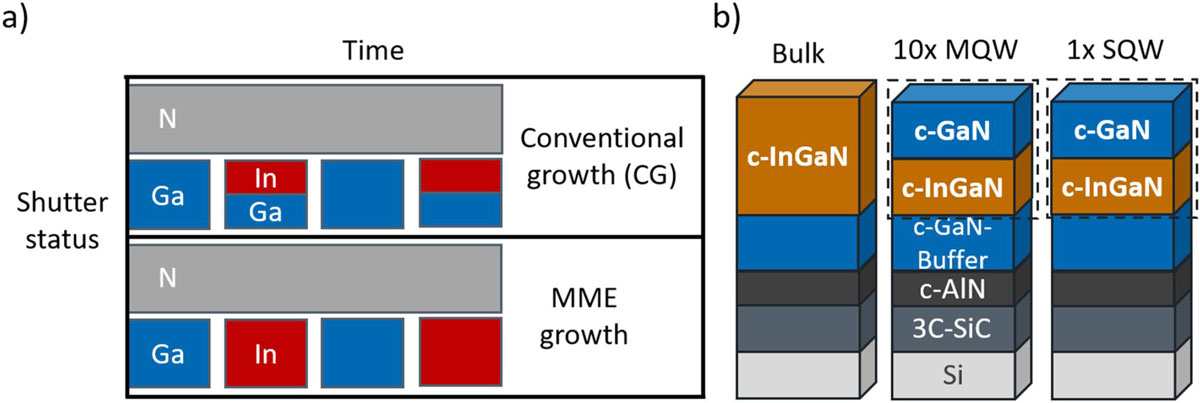
Figure 1: (a) Shutter timing for conventional and metal-modulated growth of InGaN/GaN QWs. (b) Sample structure on common buffer/substrate stack: bulk InGaN layer, InGaN/GaN 10-period MQW, and SQW.
The c-InGaN layers were grown on 600nm-thick c-GaN templates with 8nm cubic aluminium nitride (c-AlN) buffer on the substrate. The nitrogen component came from an RF plasma source.
Three growth scenarios were implemented: bulk c-InGaN, alongside 10-period multiple quantum wells (MQWs), and single quantum wells (SQWs). The bulk material was grown at 600°C, while the QWs were grown at the lower temperature of 565°C.
The researchers explain: “The lower growth temperatures for the quantum well structures cause higher indium incorporation. This compensates for the blue-shift caused by quantum confinement and compressive strain in order to achieve red emission.”
Table 1: Overview of six samples investigated.
Sample |
x (In) | Thickness (well/barrier) (nm) | PL emission energy 290 K (eV) | Roughness (nm) | Out-of-plane strain (10−3) | Hexagonal inclusions (%) |
| Bulk CG | 0.28 | 253 | 1.82 | 11.5 | 7 | 3 |
| Bulk MME | 0.28 | 245 | 1.85 | 9 | 10.8 | 0 |
| MQW CG | 0.32 | 209 (12/10) | 1.89 | 3.1 | 23.9 | 4 |
| MQW MME | 0.33 | 216 (12/10) | 1.91 | 2.5 | 20.9 | 0 |
| SQW CG | 0.32 | 22 (12/10) | 1.98 | 2.5 | 31.9 | 0 |
| SQW MME | 0.34 | 26 (15/11) | 1.92 | 1.4 | 34.3 | 0 |
A range of material characteristics were extracted from the resulting samples (Table 1). One advantage of the MME method was the elimination of hexagonal crystal structure inclusion during growth, as determined by reciprocal space mapping from high-resolution x-ray analysis. Also, the surface roughnesses were reduced. The 1.82–1.98eV photoluminescence (PL) energy range corresponds to a wavelength range of 681–626nm. This verges on the red range of 625–750nm.
The team comments: “MME remains effective for achieving red emission despite the challenges associated with higher indium incorporation >35% in MME growth, such as pore formation in bulk layers and the onset of InN formation at lower temperatures.”
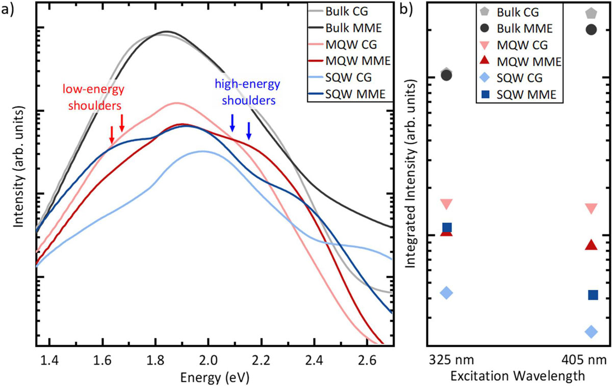
Figure 2: (a) Room-temperature PL spectra of all six samples on logarithmic scale. Selected high- and low-energy shoulders indicated by blue and red arrows, respectively. (b) Integrated PL intensity with 325nm and 405nm excitation wavelengths.
The spectral performance of the samples under PL showed the highest intensity for the bulk samples (Figure 2). The researchers comment: “While QW structures are, in principle, expected to provide enhanced radiative efficiency due to carrier confinement, the observed PL intensity of the bulk layers in our cubic InGaN samples exceeds that of the QW structures by one to two orders of magnitude.”
The team points to three factors contributing to this behavior:
1. The QWs were relatively thick, reducing the confinement effect.
2. The well/barrier interfaces introduced non-radiative recombination centers, reducing light output.
3. The effective active volume of QWs is much less than that of bulk material.
A further observation was that the MME MQW and SQW samples showed similar intensity levels overall. This was explained by the absorption of 325nm excitation (3.81eV) in the c-GaN barrier layers, exceeding the bandgap of around 3.3eV. The 325nm excitation was unable to effectively penetrate more than the top QW of the MQW structure.
Reducing the excitation energy to 3.06eV (405nm), below the bandgap, separated the SQW and MQW intensities. “As expected, the MQWs outperform the SQWs by up to about an order of magnitude for in-well pumping,” the researchers comment.
The MME QW samples showed broader spectra with pronounced shoulders on the low- and high-energy sides of the main peaks for the SQW and MQW structures, respectively. The corresponding full widths at half maximum (FWHM) were 460meV and 430meV. On the basis of this, and micro-cathodoluminescence mapping studies, the team suggests a model of potential barriers around pit-like depressions mainly caused by thinner well thickness and lower indium content at the pit’s side-walls, which spatially and energetically separate the recombination pathways for the peaks.
The researchers comment: “The emission energy stability under varying excitation is also observed for all other samples studied and represents a significant advantage of cubic InGaN structures. It highlights the absence of internal polarization fields and the resulting lack of the quantum-confined Stark effect.”
The researchers also studied the integrated intensity behavior of the main peaks of the samples, excluding any shoulders (Figure 3). This behavior gives an indication of the effects of non-radiative recombination.
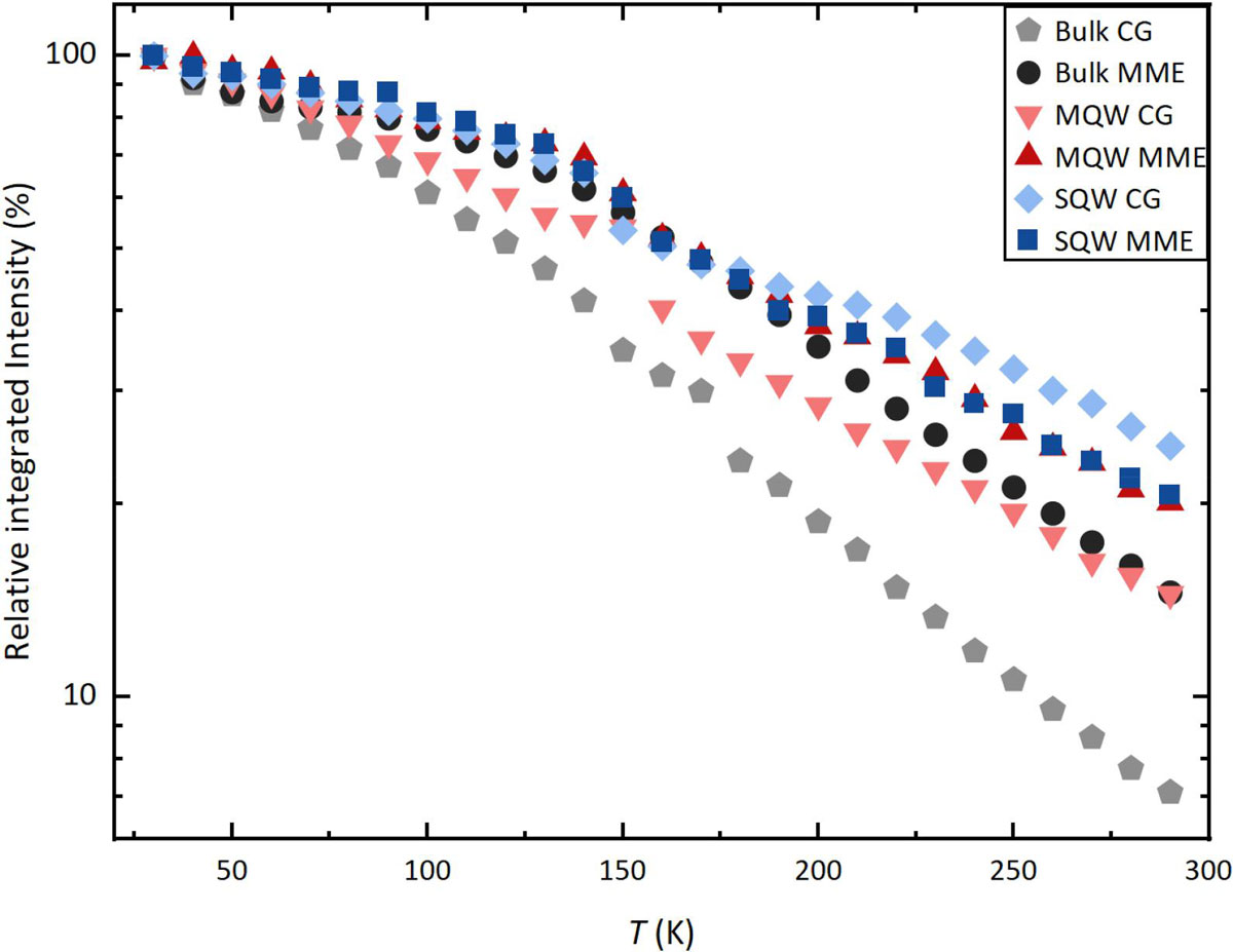
Figure 3: Relative, spectrally integrated PL intensity of main emission peak for all six samples versus temperature, normalized to respective intensity at 30K.
The researchers comment: “Non-radiative recombination centers are considered less active at cryogenic temperatures as the excited carriers do not relax toward them across the disordered potential landscape. The excited carriers gain thermal energy by increasing lattice temperature and can then increasingly access these centers. This leads to a reduction in radiative efficiency, the so-called ‘thermal quenching’.”
The bulk and MQW MME samples maintain higher integrated intensities over the CG materials at higher temperatures.
A change in slope at around 150K is associated with a switch in the main quenching mechanism from recombination at non-radiative defects at low temperature to a steeper slope for thermionic emission of carriers from the InGaN well into the GaN barrier.
The researchers report: “The strongest high-temperature quenching is observed in the bulk layers, which renders thermionic escape from InGaN into GaN as the dominant quenching pathway for temperatures above 150K unlikely. An alternative explanation is the thermal dissociation of excitons, since the exciton binding energy decreases with increasing quantum well thickness. This leads to a stronger temperature-induced quenching in bulk-like samples consistent with our observations.”
Metal-modulated epitaxy Cubic indium gallium nitride c-InGaN Red light emission LEDs
https://doi.org/10.1063/5.0305390
The author Mike Cooke is a freelance technology journalist who has worked in the semiconductor and advanced technology sectors since 1997.


