


News: Microelectronics
16 January 2026
Reducing wafer bow in GaN-on-QST growth
Imec in Belgium and Aixtron SE in Germany have reported that modifying the growth pressure during metal-organic chemical vapor (MOCVD) can reduce wafer bowing of 200mm-diameter wafers aimed at vertical gallium nitride (GaN) high-voltage devices [Kwang Jae Lee et al, Appl. Phys. Lett., v127, p241902, 2025]. Wafer bowing makes large-area device fabrication difficult, if not impossible.
Vertical devices aimed at high voltage ratings 1200V and beyond need to include thick drift layers to reduce the electric field below its critical breakdown value. Increased thickness heteroepitaxy tends to increase wafer bowing due to the different stresses in the epitaxial layers of different composition and the underlying substrate. Stress, in addition, tends to generate defects such as micro-cracks or slip lines. The wafer bow problem also becomes more critical as the wafer diameter increases.
The researchers used Qromis substrate technology (QST) wafers aimed at GaN epitaxy for high-voltage applications. The US fabless company Qromis supplies commercial 200mm wafers through partnerships with substrate foundries.
The Imec/Aixtron team comments: “The use of standard 200mm Si(111) to grow such thick GaN stacks is extremely challenging due to high risk of wafer breakage and delamination. The QST substrates with Si(111) top layer are available primarily in 200mm and in early research phase for 300mm diameter, and they consist of a poly-crystalline AlN core, which makes these substrates mechanically robust and well suited for device processing with very low risk on wafer breakage.”
The pressure modification implemented by the Imec/Aixtron team introduced sufficient build up of compressive stress during the high-temperature GaN growth that compensated for the tendency to tensile stress during cooldown.
The researchers comment: “This method is a crucial advancement for GaN vertical device development, enabling for so-far unreached wafer bow control during MOCVD processing, accommodating wider thickness variations in the drift layer and enabling large-area processing.”
For applications for 1200V and beyond, vertical device structures “offer multiple advantages including maintaining a compact device footprint, achieving higher breakdown voltages, supporting greater current-handling capacity, and delivering superior switching and dynamic performance,” according to the team.
Presently, vertical device development mainly uses bulk or freestanding GaN substrates. Such substrates are very expensive and much smaller (150mm diameter at most) than what is available for silicon. The small size adds to the expense of device fabrication.
The researchers used Aixtron’s G5+ C Planetary Reactor to grow GaN layers on five 200mm QST wafers in each run (Figure 1). The team studied the effect of reducing the growth pressure of the first undoped GaN (1st u-GaN) layer from 300mbar down to 150mbar. The second u-GaN layer was grown at 300mbar in all samples.
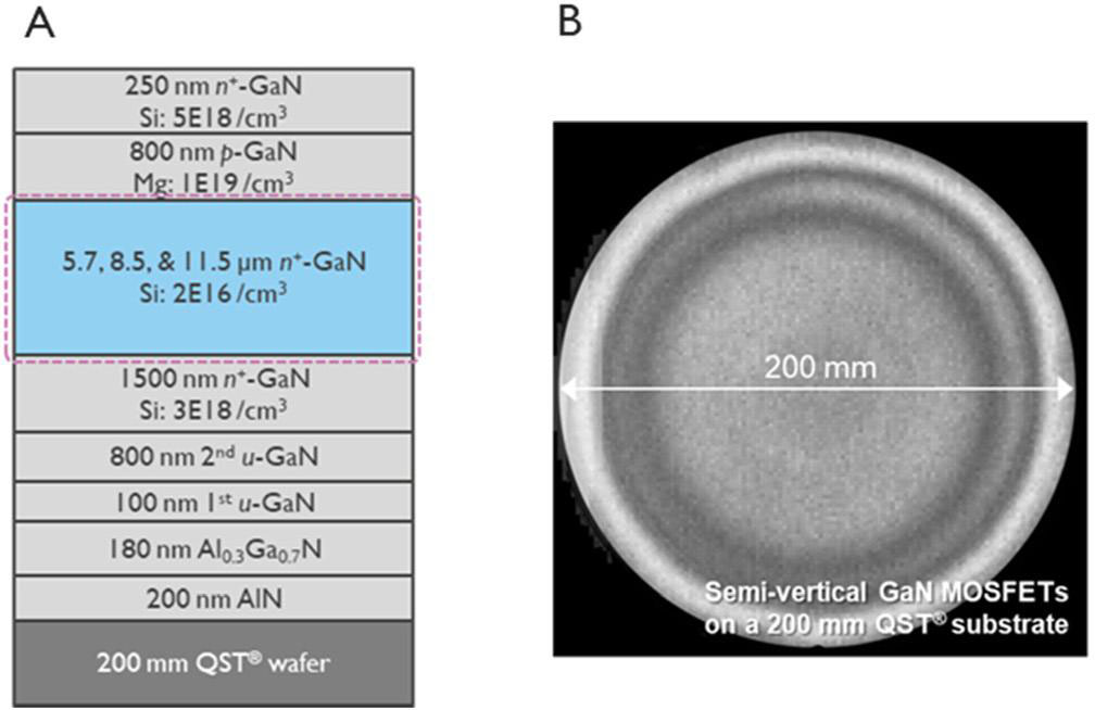
Figure 1: (a) Epitaxial stack scheme aimed at vertical GaN MOSFETs, (b) CAMTEK top-view optical image after stack growth on 200mm QST wafer.
The researchers used Gen II QST wafers, which have much lower convex initial bowing (0–50μm) relative to Qromis’ Gen I product (>100μm). Gen I wafers needed complex buffer designs, involving superlattices, to compensate for the initial bowing. Using Gen II substrates enabled a much simpler transition between the Si(111) surface of the QST wafer to the GaN layers with aluminium nitride (AlN) nucleation and AlGaN alloy buffer.
The researchers first studied 5.7μm, 8.5μm, to 11.5μm drift layers to be grown with crack-free and mirror-like surfaces with 300mbar first u-GaN layers on Gen II QST wafers. However, as the drift layer thickness increased the bow after growth also increased. At 11.5μm the wafer bow was around −85μm.
On QST wafers with zero wafer bow the final bowing could be reduced to flatness if the 1st u-GaN layer was grown at 165mbar (Figure 2).
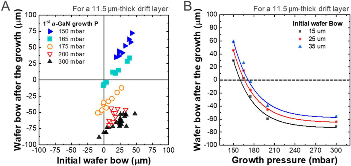
Figure 2: (a) Post-epitaxy wafer bow versus initial wafer bow for 11.5μm drift layer for different 1st u-GaN pressures. (b) Post-epitaxy wafer bow versus 1st u-GaN growth pressure.
The researchers comment: “At 150mbar, the net bow change (post–pre-Epitaxy wafer bow) shifts to positive values (compared to 300mbar), demonstrating that the net bow change can be altered from concave to convex and vice-versa simply by adjusting the growth pressure of the 1st u-GaN layer.”
The team studied in-situ reflectance measurements during the 1st u-GaN growth to assess the growth modes. At 300mbar the reflectance behavior was that of three-dimensional growth, rather than the desired two-dimensional layer-by-layer mode.
“On the other hand,” the researchers report, “the 1st u-GaN grown at 150mbar exhibits a consistent in-situ reflectance intensity from the outset, indicating that the GaN growth maintains throughout a two-dimensional (2D) growth mode.”
Raman spectroscopy analysis gave calculated residual stress in vertical GaN stacks with 11.5μm drift layers of 0.047GPa (tensile) and −0.024GPa (compressive) for 300mbar and 150mbar 1st u-GaN pressures, respectively.
The researchers add: “It was found that there is no impact on crystalline quality or the background impurity concentration within the u-GaN and the critical drift layer region.”
https://doi.org/10.1063/5.0312962
The author Mike Cooke is a freelance technology journalist who has worked in the semiconductor and advanced technology sectors since 1997.


