


News: Optoelectronics
10 February 2026
Continuous-wave AlGaN UV-A laser diode
Ohio State University in the USA has claimed the first demonstration of continuous-wave (CW), electrically pumped aluminium gallium nitride (AlGaN) ultraviolet-A (UV-A, 315–400nm) laser diodes grown monolithically by plasma-assisted molecular beam epitaxy (PAMBE) [Arnob Ghosh et al, Journal of Lightwave Technology, published online 14 January 2026].
UV laser diodes and LEDs are being developed for a wide range of potential deployments: air and water purification, disinfection, sterilization, fluorescence-based biological detection, microfabrication, and various biotechnology processes. Optoelectronic UV sources offer many advantages related to compact size, relatively high energy efficiency, and reduced manufacturing cost. The applications prefer CW over pulsed-mode operation.
The researchers comment: “It is worth noting that most of the previously reported results were obtained under pulsed conditions, whereas this work was performed under CW operation, representing more stringent and practically relevant operating conditions.”
A leading disadvantage of AlGaN alloy semiconductor material is the difficulty in achieving hole injection, since conventional p-doping with magnesium has low carrier concentration efficiency. The OSU device used a transparent buried tunnel junction (TJ) enabling hole injection into the quantum-well active region, despite the top cladding being composed of n-type AlGaN.
The team explains: “The device structure features a transparent homojunction tunnel junction to enhance hole injection, along with a narrow-ridge, index-guided asymmetric waveguide design that significantly improves optical confinement while minimizing absorption losses from the substrate.”
The researchers plan in future work to optimize design and growth on low-dislocation, high-Al-content AlGaN or AlN substrates to extend emission into the shorter-wavelength, and even more challenging, UV-B (280–315nm) and UV-C (100–280nm) spectral regions.
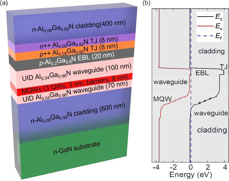
Figure 1: (a) Cross-sectional schematic of designed planar UV-A AlGaN laser structure, and (b) corresponding energy-band diagram in thermal equilibrium.
The epitaxial material for the laser diode was grown on c-plane free-standing GaN substrates (Figure 1). The structure included an electron-blocking layer (EBL) to suppress electron overflow from the active region. The tunnel junction for hole injection into the multiple quantum wells (MQWs) consisted of thin heavily doped layers of p++- and n++-type AlGaN.
The layer thicknesses were carefully designed to ensure a high optical confinement factor at the MQW. In particular, a thick bottom cladding was designed to compensate for the relatively high refractive index of the n-GaN substrate, which otherwise would tend to pull the optical mode downward, resulting in increased parasitic absorption in the substrate. The waveguide thicknesses were also chosen with this in mind.
The researchers comment: “This configuration effectively redirects the optical field away from the lossy GaN substrate and improves mode overlap with the QWs.”
The material was fabricated into 3μm-wide ridge waveguide lasers. The cleaved cavity length was 500μm. The ridge was formed by inductively coupled plasma reactive-ion etching (ICP-RIE) to a depth of 420nm. The ridge was designed to enhance lateral confinement of the optical field in the QW region.
The ohmic top-side contacts were applied to the n-AlGaN cladding, consisting of annealed titanium/aluminium/nickel/gold.
The lasers were also passivated with plasma-enhanced chemical vapor deposition (PECVD) silicon dioxide. The bottom contact metals were the same as for the top side, applied after thinning the device to 140μm. Nickel/gold contact pads were also formed. The characterization tests were on unpackaged devices without optical coatings of the facets.
The lasers, in CW operation, achieved 6kA/cm2 threshold current density (Jth) at 8.5V forward bias (Figure 2). The total differential external quantum efficiency (DEQE, ηd) was 11%.
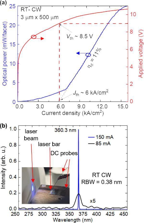
Figure 2: (a) Light output power–current–voltage (L-I-V) characteristics of Fabry–Pérot laser, and (b) emission spectra at below- and above-threshold with emission profile inset. Spectrometer resolution bandwidth (RBW) was 0.38nm.
The team comments: “The ηd is expected to improve significantly with the incorporation of dielectric mirror coating on the facets and proper thermal management via packaging.”
The subthreshold (85mA) peak wavelength was 361nm with 8nm full-width at half maximum (FWHM). Above threshold (150mA), the wavelength was 360.3nm (0.5nm FWHM, close to resolution limit).
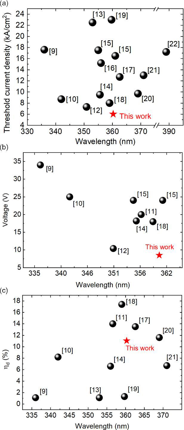
Figure 3: Benchmark comparisons of (a) threshold current density, (b) operating voltage and (c) ηd of presented CW device with other reported UV-A laser diodes under pulsed-mode operation.
The researchers compared the performance of their CW UV-A laser diode with reports of pulse-mode performance in the engineering literature (Figure 3): “The data clearly demonstrate that this work achieved a record low threshold voltage and current density, primarily attributed to the implementation of a homojunction TJ and an improved cavity design.”
AlGaN UV-A laser diode AlGaN PECVD GaN substrate
https://doi.org/10.1109/JLT.2026.3654012
The author Mike Cooke is a freelance technology journalist who has worked in the semiconductor and advanced technology sectors since 1997.


