
News: LEDs
7 August 2026
Reducing micro-LED sidewall impact
Researchers based in China have reported 34% enhanced external quantum efficiency (EQE) of a 5μm gallium nitride (GaN) blue light-emitting diode (LED) from a neutral reactive nitrogen/hydrogen (N/H) treatment [Kai Li et al, Appl. Phys. Lett., v129, p032103, 2026].
The team from University of Science and Technology of China, Suzhou Institute of Nano-tech and Nano-bionics, and Jiangsu Institute of Advanced Semiconductors, reports: “Treatment of neutral reactive N/H species effectively mitigates the surface Fermi-level pinning and reduces the defect-related surface states. This step is directly followed by vacuum-interconnected atomic layer deposition (ALD) passivation, preventing air exposure and secondary impurity adsorption.”
The use of neutral N/H radicals also has the advantage of avoiding surface charging, generating strong local electric fields, and consequent anomalous band bending at the sidewalls.
Micro-LEDs are particularly sought for next-generation high-resolution displays and for communication technologies due to high brightness, high efficiency, fast response, and long operational lifetime. However, micro-LEDs suffer from increased sidewall negative impacts due to the perimeter/area ratio scaling inversely with size.
Conventional methods to reduce sidewall defects and efficiency losses often involve etching the surface back. This can smooth the surface, making it more liable to reflect light back into the device, reducing the light extraction efficiency.
Device fabrication (Figure 1) began with commercial blue LED epitaxial material consisting of silicon-doped n-GaN, 20 cycle strain release layer (SRL), six pairs of multiple quantum well (MQW), and magnesium-doped p-GaN. Indium tin oxide (ITO) was added by magnetron sputtering to encourage current-spreading.
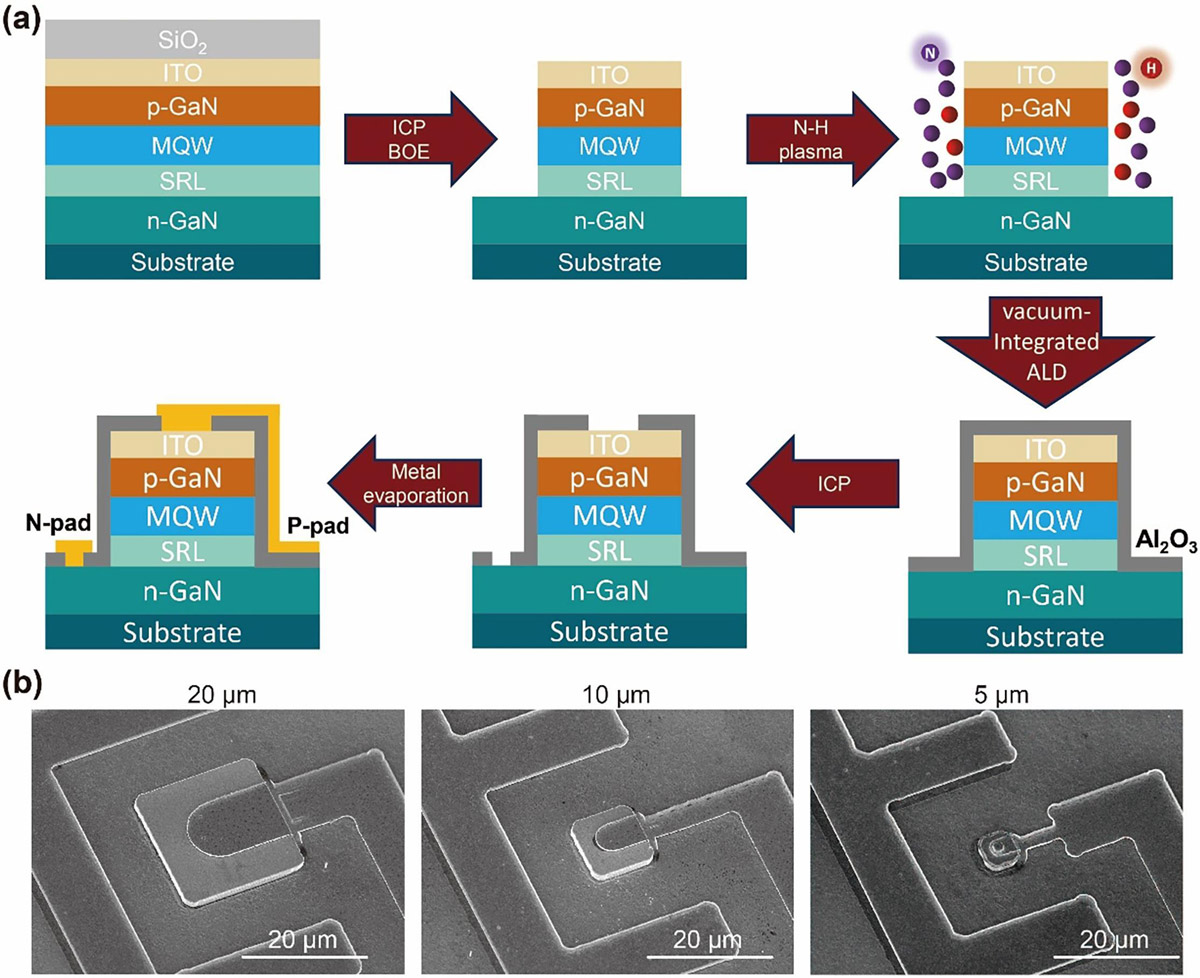
Figure 1: (a) Fabrication process for micro-LED chip arrays. (b) SEM images of micro-LED chips with various sizes.
The device mesa was etched by inductively coupled plasma (ICP) with a silicon dioxide (SiO2) layer used as a mask. The mask was removed by buffered oxide etching (BOE).
The sidewall was repaired by exposure to radio frequency (RF) sourced nitrogen/hydrogen (N/H) radicals. The material was then transferred to an ALD chamber in vacuum to avoid oxidation and other secondary contamination of the sidewall. The ALD process was used to apply 30nm aluminium oxide (Al2O3) as sidewall passivation.
The titanium/aluminium/nickel/gold metal electrodes were deposited through ICP-etched contact vias.
The impact of the sidewall treatment was most significant on the smallest 5μm LED: the peak external quantum efficiency (EQE) increased to 18.52% from 13.76%, an increase of 34.6%. The larger devices benefited to a lesser extent: from 26.92% to 29.71%, and from 24.63% to 28.13%, for the 20μm and 10μm LEDs, respectively.
The reverse current leakage at −5V was also significantly reduced by up to five orders of magnitude: from 7.53×10⁻³A/cm2 to 6.37×10⁻⁷A/cm2, from 8.44×10⁻²A/cm2 to 2.26×10⁻⁶A/cm2 and from 1.30A/cm2 to 9.64×10⁻⁶A/cm2 for the 20μm, 10μm and 5μm devices, respectively. Also, the treatment eliminated a low-forward-bias hump in the current–voltage characteristics. This enhanced current–voltage performance is credited to suppression of etching-induced leakage by the N/H radical treatment.
The researchers add: “These improvements are attributed to the reduced sidewall carrier loss, non-radiative recombination, and shunt leakage paths, which are especially critical in smaller micro-LEDs because of their larger surface-to-volume ratio.”
Secondary-ion mass spectrometry (SIMS) analysis showed reduced levels of fluorine (F), chlorine (Cl), and carbon (C) after the N/H treatment. The researchers comment: “The decrease in carbon concentration is due to the removal of adventitious hydrocarbons/organic residues introduced during air exposure. chlorine residues associated with Cl-based plasma etching and fluorine residues introduced during HF stripping of the SiO2 hard mask can be effectively removed during N/H treatment.”
In particular, the hydrogen reacts with the halogens F/Cl, while the nitrogen combines with under-coordinated surface gallium sites generated after the halogen extraction from the surface.
The team explains: “This synergistic process suppresses N-vacancy- and Ga-rich-related defects and contributes to the recovery of the surface stoichiometry and electronic structure of GaN.”
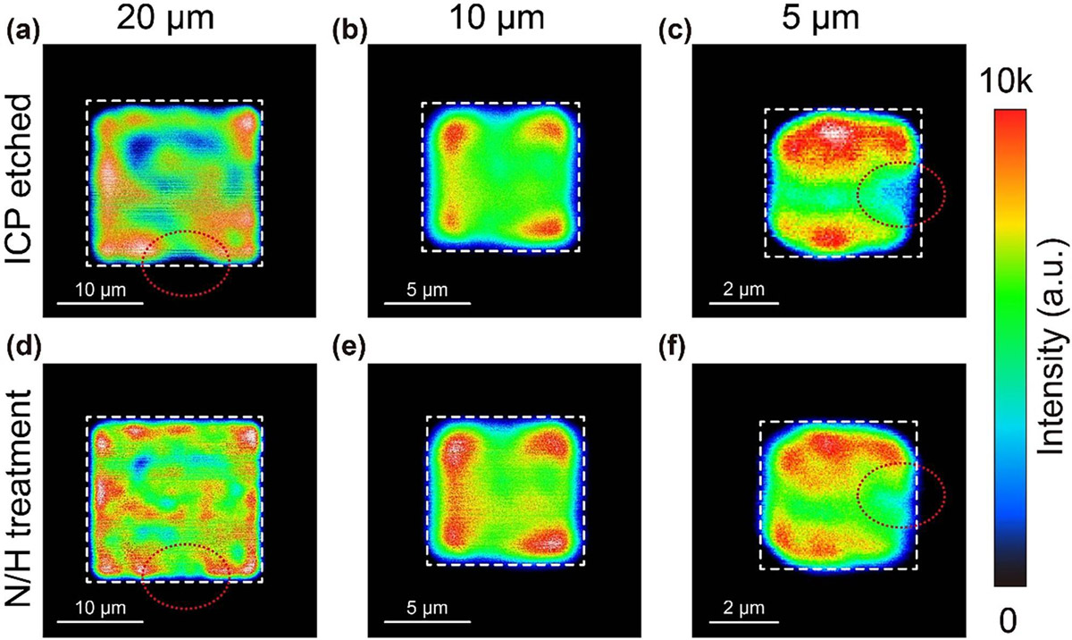
Figure 2: Laser scanning confocal microscopy (LSCM) images of micro-LEDs before (a–c) and after (d–f) neutral N/H radical treatment. Mesa sizes: 20μm (a, d) 10μm (b, e), and 5μm (c, f).
The N/H treatment was found to be effective in increasing emission, particularly in ‘dead zone’ regions (Figure 2, dotted circles).
https://doi.org/10.1063/5.0333059
The author Mike Cooke is a freelance technology journalist who has worked in the semiconductor and advanced technology sectors since 1997.