

News: LEDs
5 August 2026
Gate-all-around InGaN nano-LED
University of Michigan Ann Arbor in the USA reports a gate-all-around (GAA) nanoscale light-emitting diode (nano-LED), with a conformal gate electrode surrounding both the n-GaN contact region and the InGaN/GaN multiple-quantum-well (MQW) active region [Yakshita Malhotra et al, Optics Express, v34, p23712, 2026].
The researchers comment: “To the best of our knowledge, this is the first report of vertical integration of a field-effect transistor (FET) with a nanopillar LED in nanoscale. Further, other reports on monolithic integration of FETs with LED report much higher values of gate potential (VG−N) to manipulate the electroluminescence (EL) from LEDs.”
The team adds: “The inclusion of a third electrode is not only handy in terms of monolithic vertical integration of a FET with an LED, but it can also be used to modulate the surface recombination properties and overall enhancement of the radiative recombination efficiency, which is one of the major challenges for making high efficiency submicron-scale LEDs.”
Surface non-radiative recombination mechanisms tend to become more significant as device sizes shrink. The researchers see the structure as “a promising route for achieving high-efficiency nanowire LEDs and large-scale three-dimensional optoelectronic integration”.
Without the gate (Figure 1), the nano-LED pillar suffers from surface recombination where electrons and holes are absorbed through transitions to intermediate levels that do not produce the desired photons, the Shockley−Read−Hall (SRH) mechanism. These intermediate levels arise from damage such as dangling bonds and surface defect states caused by the plasma etch used to create the pillars.
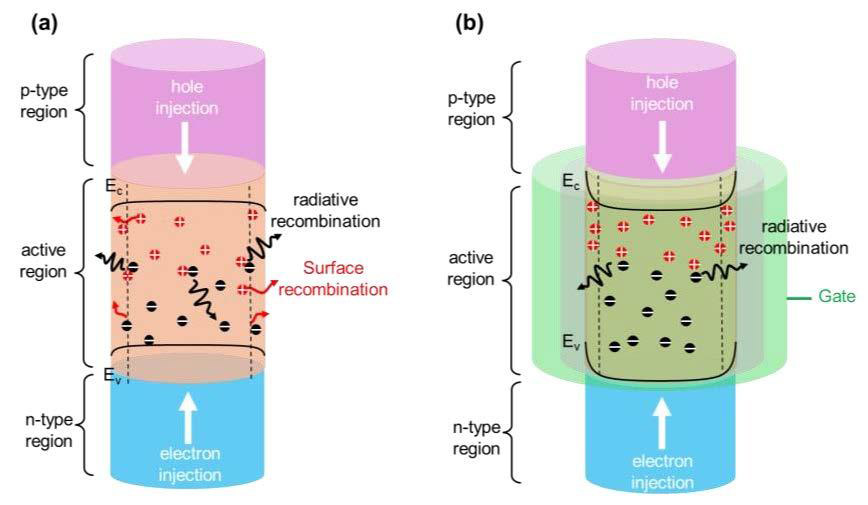
Figure 1: (a) Recombination mechanisms in conventional two-terminal LED. (b) Gated structure used to alter balance of recombination towards photon production.
A negative potential applied to the gate confines the electrons away from the surface, enabling more transitions across the bandgap of the multiple quantum wells. The holes on the other hand will be attracted to the surface column, but they travel more slowly, and will lack electrons to absorb there.
A positive gate potential would attract the electrons to the surface region, reducing light emission compared to non-radiative mechanisms.
The gate in the Michigan devices also covered the n-type GaN electron injection region, giving a field-effect transistor (FET)-like operation profile. Commenting on simulations, the researchers write: “The current injection is controlled primarily by the accumulation and depletion of electrons in the n-GaN layer.”
The researchers used commercial GaN-based epitaxial wafers grown on silicon (Si) (111) substrates for fabrication of the GAA nano-LEDs (Figure 2). The structure consisted of 2800nm n-GaN, 160nm active region of InGaN/GaN multiple quantum wells (MQWs), and 150nm p-GaN.
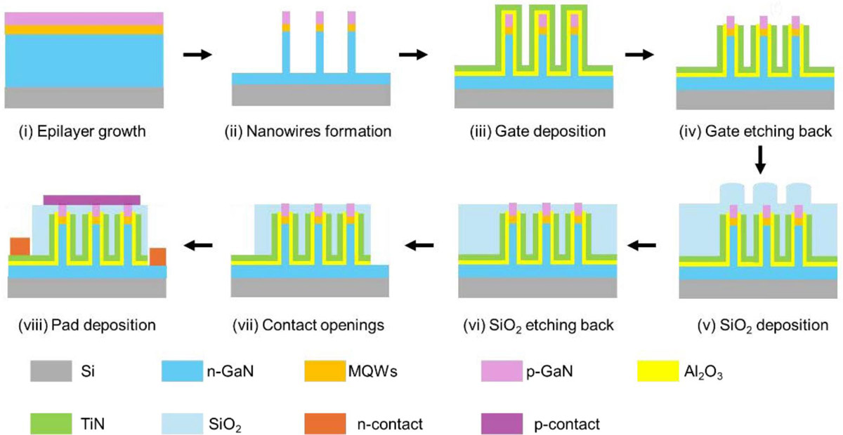
Figure 2: GAA LED fabrication process.
The material was etched into hexagonal arrays of 220nm-diameter nanopillars down to the n-GaN layer. The gate stack consisted of 30nm atomic layer deposition (ALD) aluminium oxide (Al2O3) dielectric, and 75nm titanium nitride (TiN) metal. The gate material was removed from the top 100nm of the nano-pillars by etch-back. The gate thus surrounded the n-GaN and active region.
A 600nm silicon dioxide (SiO2) layer was applied through plasma-enhanced chemical vapor deposition (PECVD), insulating the gate from the p-electrode. Further etch-back exposed the p-electrodes. The metals for the n-contact and gate were titanium/gold. The p-contact was 200nm transparent indium tin oxide (ITO), 5nm nickel, and 5nm gold. The completed devices were annealed at 450°C for a minute in forming gas.
The EL of the GAA nano-LEDs was found to be fully suppressed when VG−N reached −1V (Figure 3). A positive gate potential enhanced the EL by allowing more current to flow through the device. However, as the P−N bias increased from 6V to 7V, the modulation in EL was reduced probably due to the increased non-radiative recombination at the sidewall regions.
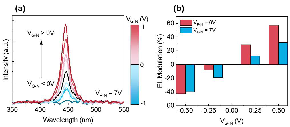
Figure 3: (a) Electroluminescence (EL) at 7V forward bias (VP−N) with varying gate potential (VG−N), 0.25V steps. (b) EL modulation versus VG−N at 6V and 7V VP−N.
To get a better idea of the quantum efficiency (QE, photons/electron injected) performance, the researchers studied the integrated EL performance against current density for different gate potentials (Figure 4). Dividing the integrated EL by the current density gave a qualitative ‘quantum yield’, proportional to the QE, allowing the relative comparison of performance under different gate conditions.
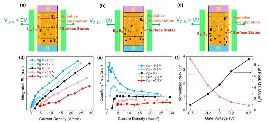
Figure 4: Schematics showing impact of gate bias on band diagrams and defect states: (a) VG−N < 0V (b) VG−N = 0V and (c) VG−N > 0V. (d) Integrated EL versus current density for different VG−N. (e) Quantum yield (QY) versus current density. (f) Normalized peak QY (red curve) and current density (black curve) versus VG−N.
The researchers report: “The peak QY shows an enhancement of almost 4 times at VG−N = −0.5V. On the other hand, for Vg > 0V, the QY is significantly reduced to 0.35 times at VG−N = +0.5V. For an LED, a slow rising QE, reaching its peak at higher current densities, is a typical indication of a large non-radiative recombination component related to defect related SRH recombination. Whereas a sharp rise to peak QE at low current densities indicates reduced SRH recombination.”
https://doi.org/10.1364/OE.588188
The author Mike Cooke is a freelance technology journalist who has worked in the semiconductor and advanced technology sectors since 1997.