

News: Microelectronics
7 August 2026
GaN HEMT short-circuit performance
Researchers based in China claim record short-circuit (SC) performance for 650V Schottky p-GaN high-electron-mobility transistors (HEMTs) [Ning Yang et al, IEEE Transactions on Power Electronics, published online 9 July 2026]. In particular, the device achieved a record SC withstand time (tSC) of 629μs under a single stress event, and was also capable of withstanding up to 12,000 repetitive SC cycles of pulses up to 50μs duration.
The team from University of Electronic Science and Technology of China (UESTC) and Shenzhen Pinghu Laboratory attribute the improved SC capability to the use of a thinner-than-usual aluminium gallium nitride (AlGaN) barrier layer. The thinner barrier allows electrons from the channel to flow into the gate electrode during short-circuit events, adaptively reducing the gate potential, and thus partially pinching off the two-dimensional electron gas (2DEG) channel. The negative feedback reduces the drain current, mitigating self-heating effects responsible for device burnout.
The researchers see the enhanced SC robustness as enabling increased market penetration for GaN power HEMTs beyond consumer electronics applications (e.g. fast chargers) into industrial power conversion, automotive power-trains, renewable energy applications, and motor drives.
The team comments: “Short-circuit robustness of GaN HEMTs has emerged as a critical reliability concern in these applications. SC events, caused by accidental load shorting or external faults, subject devices to concurrent high drain-source voltage and current, generating excessive transient power that can induce severe degradation or catastrophic failure. This intrinsic weakness under SC stress remains a major barrier to the broader deployment of GaN HEMTs in high-reliability power electronics.”
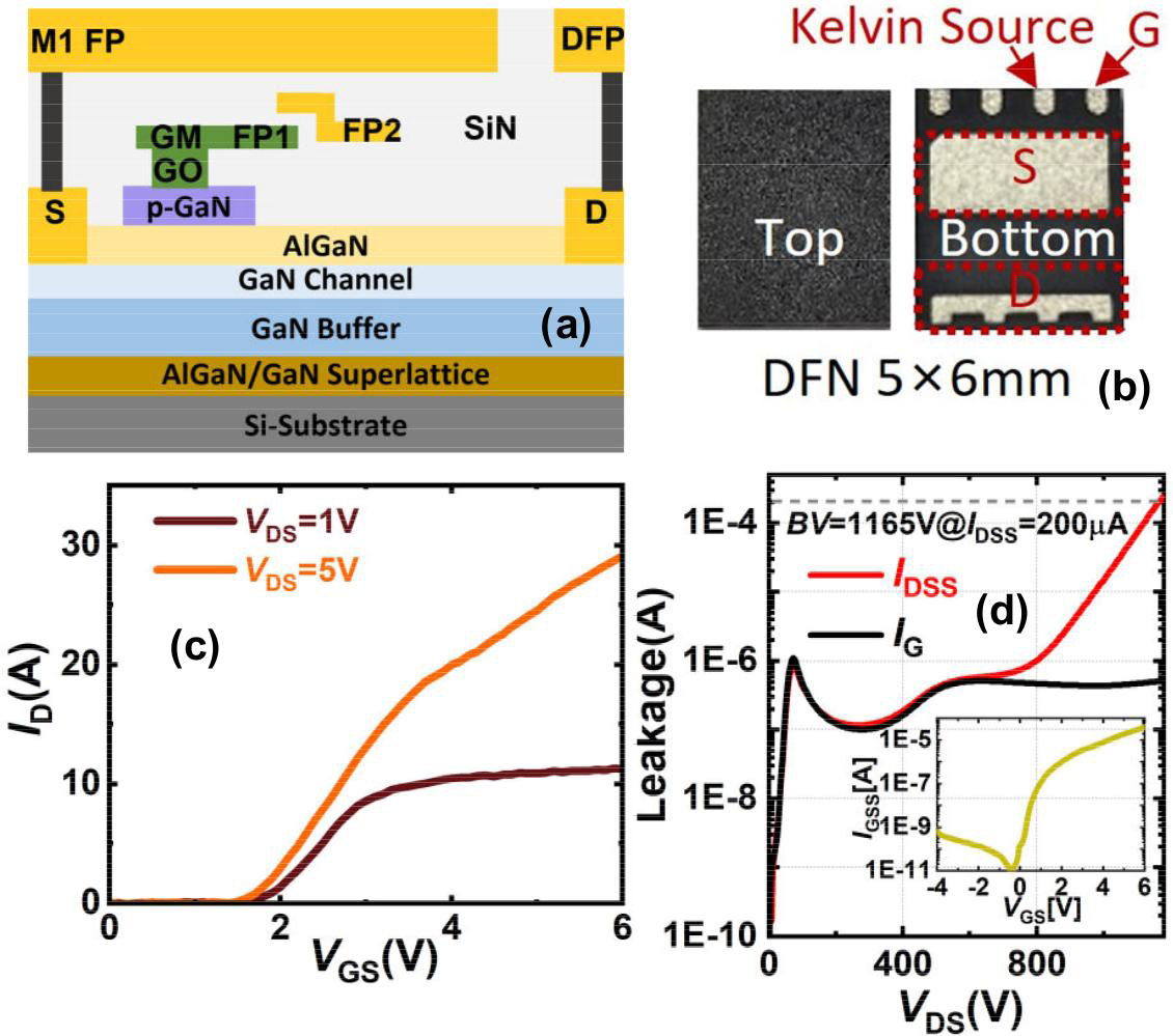
Figure 1: (a) Cross-sectional schematic of 650V enhancement (E)-mode GaN HEMTs. (b) Top and bottom views of packaged device. (c) Transfer curves, drain current (ID) versus gate potential (VGS) at 1V/5V drain biases (Vds). (d) Off-state gate (IGSS) and drain (IDSS) leakage currents versus Vds.
The epitaxial material for the device consisted of 6-inch silicon (Si) substrate, 2.85μm AlGaN/GaN superlattice transition layer, 1.96μm GaN buffer/channel, 11nm AlGaN barrier, and p-GaN gate (Figure 1). The gate length was 1.42μm. The fabricated device featured a number of field plates (FPs) to enable high-voltage operation by optimizing the the electric field distribution. The devices were encapsulated into dual flat no-lead (DFN) packages for testing.
The off-state breakdown voltage (BV) for a 200μA drain leakage current was 1165V. The operating characteristics included 31A saturation current at 6V gate potential, 1.15V threshold, and 89mΩ on-resistance, comparable with typical commercial devices aimed at 650V/150mΩ and 700V/106mΩ operation.
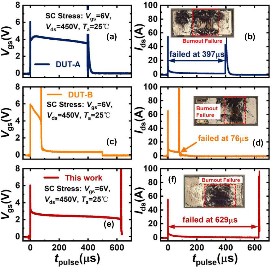
Figure 2: Single-pulse SC voltage (left) and current (right) waveforms with 450V drain stress and 6V gate potential: commercial comparison devices under test DUT-A (a, b) and DUT-B (c, d), along with Yang et al’s device (e f).
Under single-pulse short-circuit stress, the device achieved a claimed record withstand time (tSC) of 629μs, almost doubling that of the best of the comparison devices under test (Figure 2). Increasing the drain bias to 500V and 550V, the team found the tSC of its device reduced somewhat to 436μs and 337μs, respectively. At 550V, the comparison devices DUT-A and DUT-B only managed 0.245μs and 0.19μs, respectively.
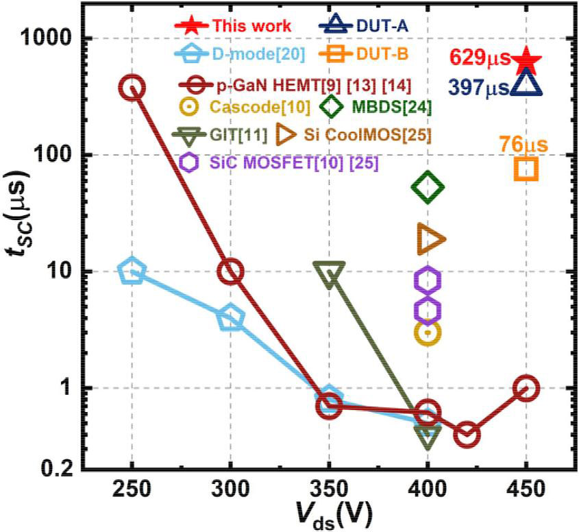
Figure 3: Benchmark of single-pulse SC capability: tSC versus Vds for 600–650V GaN power HEMTs, 650V silicon CoolMOS and 650V SiC MOSFETs.
The researchers also present a more extensive comparison against other reports, including silicon and silicon carbide (SiC) power transistors under various Vds stresses (Figure 3).
The team’s device also showed superior performance under repeated shorter stress events (Figure 4). The researchers report: “Both commercial devices, DUT-A and DUT-B, failed at the third SC cycle, whereas the proposed device survived after 12,000 cycles repetitive SC stress events without device failure. Furthermore, even under a much longer SC pulse width of 50μs, the proposed device is still capable of withstanding 12,000 cycles repetitive SC stress without failure.”
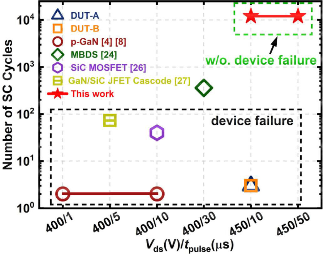
Figure 4: Benchmark of repetitive SC capability: Vds/tpulse versus SC cycles for 650V GaN HEMTs, 650V GaN/SiC JFET cascode and 1.2kV SiC MOSFET.
The endurance under the longer 50μs pulses is the first such report for GaN power devices, according to Yang et al.
https://doi.org/10.1109/TPEL.2026.3711894
The author Mike Cooke is a freelance technology journalist who has worked in the semiconductor and advanced technology sectors since 1997.