

News: Optoelectronics
5 August 2026
First continuous-wave UV VCSEL operation at room temperature
Researchers based in China claim the first gallium nitride (GaN)-based electrically injected continuous-lasing ultraviolet (UV) vertical-cavity surface-emitting laser (VCSEL), achieved by “careful design and processing” [Zhi-Jie Zou, et al, Appl. Phys. Lett., v128, p253501, 2026].
“Until now, GaN-based UV VCSELs have been demonstrated under optical pumping, but there are still no electrically injected VCSELs with lasing wavelength shorter than 402nm,” reports the team from Xiamen University, Institute of Semiconductors, and Southern University of Science and Technology (SUSTech).
The research focused on reducing optical losses, and improving the thermal performance of the device. The researchers report: “These efforts allowed us to realize the UV VCSEL lasing at room temperature at a wavelength of 380.1nm and a threshold of 14.9kA/cm2.”
The team hopes that their work will contribute to more successful UV GaN laser deployment for biological regulation, sterilization, disinfection, medical treatment, and UV curing.
The UV VCSEL (Figure 1) included double dielectric distributed Bragg reflectors (DBRs). The III-nitride epitaxial material was grown on c-plane sapphire through metal-organic chemical vapor deposition.
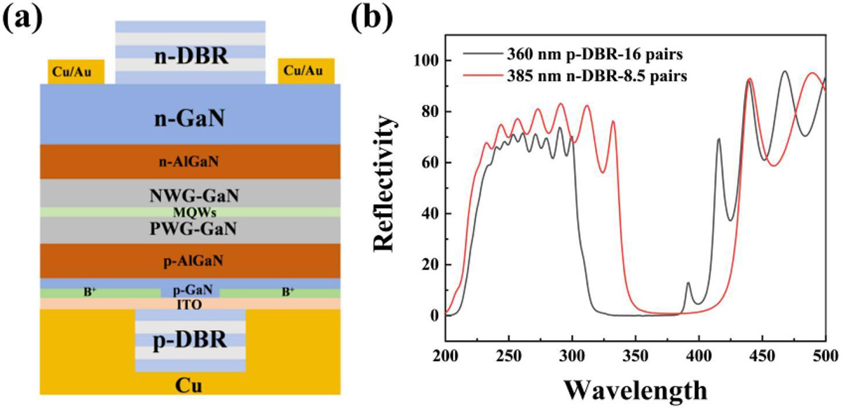
Figure 1: (a) UV VCSEL structure and (b) reflectivity spectra of DBRs.
The cladding was aluminium gallium nitride (AlGaN) layers contained 5% aluminium on the n-side and 4.5% on the p-side. These cladding layers were both 600nm thick. The doped GaN waveguide (WG) layers were both 150nm. The active light-generating region consisted of a multiple quantum well (MQW) stack consisting of indium gallium nitride (In0.05Ga0.95N) wells and GaN barriers.
The epitaxial material was prepared for the laser fabrication by laser lift-off removal of the sapphire substrate and chemical mechanical polishing to smooth the exposed n-GaN surface from 1.71nm to 0.24nm roughness. This was expected to reduce interface scattering loss from 3.26% to 0.07%, thus decreasing the gain threshold for lasing.
The laser cavity was defined by two dielectric hafnium oxide and silicon dioxide (HfO2/SiO2) DBR reflecting structures. The p-side contained 16 layer pairs, and the n-side contained 8.5. The center wavelengths for transmission were 360nm and 385nm for the p-side and n-side, respectively. The cavity length was about 4μm.
The researchers report: “The difference in the center wavelength is due to the unstable growth parameters. At 380nm, the transitivity is 0.195% for the p-DBR and 0.777% for the n-DBR. The overlap region of the low-transitivity bands covers the wavelength range of the epitaxial quantum well peak (365–385nm). Consequently, the deviation in the DBR center wavelengths does not significantly affect the quality of resonant cavity.”
The 8μm-diameter current-injection aperture was confined by ion implants of boron (B). The DBR structures were etched using inductively coupled plasma. Indium tin oxide (ITO) was used as a (relatively) transparent current-spreading layer. The copper heatsink structure was applied by electroplating. The n- and p-electrodes were both chromium/gold (Cr/Au).
The designed emission wavelength was in a region where the light absorption of ITO rapidly increases, and thus it was desired to make this layer as thin as possible; this layer was 20nm in the reported device, compared with the ~50nm typically used in blue VCSELs.
Also, HfO2 was used as an optical adjustment layer with the aim of putting the ITO at a node and the MQW at an anti-node of the optical field: i.e. the ITO was placed at a position of minimum electromagnetic oscillation and the MQW at a maximum.
The lasing wavelength of the device red-shifted by 0.38nm as the bias power increased from 37.8mW to 126.3mW (Figure 2). The slope of a linear fit was 4.52nm/W. Increasing the ambient temperature of the device also red-shifted the wavelength at a rate of 0.0216nm/K. The thermal resistance was estimated at 209K/W (4.52/0.0216).
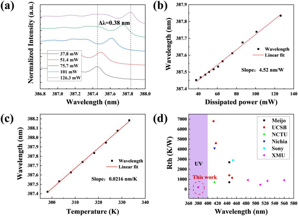
Figure 2: (a) Normalized electroluminescence (EL) spectra at different bias powers. Variations of wavelength with (b) dissipated power and (c) device temperature; (d) thermal resistance versus wavelength comparisons of GaN-based resonant-cavity light-emitting devices in research literature.
The researchers comment: “The lower thermal resistance indicates better heat dissipation capability, which is attributed to the use of the B+-implanted layer and the electroplated copper plate.”
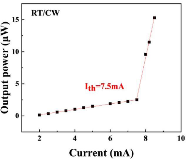
Figure 3: Output power versus injection current.
The continuous wave (CW) threshold current (Ith) at room temperature (RT) was 7.5mA (14.9 kA/cm2), evidenced by an increase in slope of the output power curve (Figure 3).
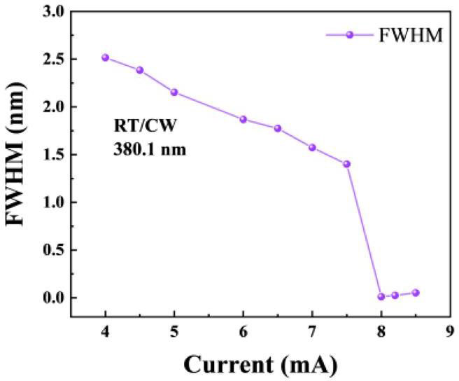
Figure 4: Evolution of full-width at half-maximum (FWHM) of 380.1nm peak with injection current.
The main peak at 380nm also significantly narrowed in the region of the threshold (Figure 4). At 8.2mA injection the FWHM was 28pm. A second cavity mode was observed at 375nm wavelength. The electrical diode characteristics include a 4.3V turn-on, and ~10−8A reverse current leakage.
https://doi.org/10.1063/5.0326228
The author Mike Cooke is a freelance technology journalist who has worked in the semiconductor and advanced technology sectors since 1997.