

News: Microelectronics
13 August 2026
Electrochemical GaN HEMT exfoliation
Researchers based in China present an electrochemical etching (ECE) technique for high-quality transfer of gallium nitride (GaN) high-electron-mobility transistor (HEMT) thin films from silicon substrate to temporary substrates [Chenxi Xu et al, J. Phys. D: Appl. Phys., v59 p315101, 2026].
The team from ShanghaiTech University, Suzhou Institute of Nano-Tech and Nano-Bionics (SINANO), and University of Science and Technology of China, comment: “Unlike conventional mechanical grinding, this method avoids mechanical damage to the device, thereby preserving the structural integrity and electrical properties of the heterostructure.”
The researchers see the technique as being a wafer-scale and low-damage route to high-quality flexible GaN HEMT thin-film applications such as next-generation flexible wireless communication systems, wearable sensing platforms, curved displays, and conformal RF electronics. At the same time, the peeled-off silicon substrate was very smooth with around 1nm surface roughness potentially allowing reuse — unlike conventional grinding and wet etching approaches.
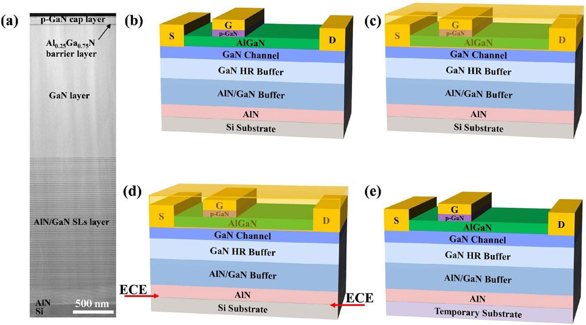
Figure 1: (a) Cross-sectional transmission electron microscope (TEM) image of epitaxial material. (b) AlGaN/GaN HEMT structure grown on silicon substrate, (c) coated with photoresist, (d) electrochemical etching lift-off of silicon substrate, (e) transfer to temporary substrate.
The epitaxial material was grown on p-type silicon (p-Si) substrate using metal-organic chemical vapor deposition (Figure 1). The aluminium gallium nitride (AlGaN) barrier layer contained 25% Al. HEMT devices were fabricated by removing the p-GaN cap except in the gate (G) region with inductively coupled plasma etching. The source (S) and drain (D) titanium/aluminium/titanium/gold metals were recessed into the barrier layer. The gate consisted of a Schottky contact of titanium to p-GaN.
The HEMTs featured 1000μm×3μm gates. The gate-to-source and -drain spacings were 4μm and 15μm, respectively.
The two-dimensional electron gas (2DEG) channel under the gate was depleted due to the p-GaN pushing the conduction band above the Fermi level. The resulting HEMT thus had a normally-off characteristic, often denoted as enhancement-mode operation. Many applications prefer normally-off transistor operation with respect to reduced power consumption and for fail-safe circuit protection, particularly in high-voltage and high-power systems.
For the electrochemical etching, the devices were protected by a 6μm layer of photoresist. The devices served as the anode of the etch process, while the cathode consisted of platinum. The electrochemical etch solution was nitric acid. The applied voltage was around 8V. This had been found to ensure a stable etching process and prevented generated reaction gas from damaging the thin film’s structural integrity.
The researchers report: “If the voltage was much lower than 8V, the entire electrochemical etching process would take an excessively long time, damage the protective photoresist and result in etching of the contact metals on the sample. Meanwhile, an excessively high voltage was also undesirable. Intense electrochemical reactions would generate many bubbles and induce substantial stress, which would further cause cracking of the released HEMT film.”
The etch process released the silicon substrate from 1cm×1cm samples in about 25 minutes. The AlN nucleation layer of the epitaxial structure is naturally heavily doped n-type near the AlN/Si interface through the diffusion of silicon atoms from the substrate during the high-temperature deposition process. This, along with strong charge polarization effects, creates a highly conductive 2DEG near the interface. The electrochemical oxidation of the III-nitride material occurs preferentially at this conductive layer.
The researchers comment: “In the electrochemical etching process, holes accumulated at the interface between AlN and the electrochemical solution, and gas evolution is subsequently detected at both the anode and cathode, indicating the generation of nitrogen and hydrogen, respectively.”
The researchers also report that the AlGaN/GaN HEMT membrane exhibits a slight curvature due to the release of internal stress from removal of the silicon substrate. On the basis of their work, they believe that the lift-off method is capable of wafer-scale substrate removal while maintaining structural integrity.
Atomic force microscopy (AFM) of the separated surfaces gave root-mean-square roughnesses of 1.9nm and 1.1nm for the thin-film and silicon substrate, respectively. “A smooth interface is highly desirable to fabricate high-performing devices,” the team comments.
Raman spectroscopic analysis found that the release resulted in a 71.4MPa relaxation in compressive stress perpendicular to the c-axis of the GaN layer.
The released thin-film HEMT structure was transferred on hydrophobic Teflon spatulas to a bath of deionized water and acetone. The Teflon avoided any tendency for the films to fold during the transfer.
The membranes were also rinsed in isopropanol and dried in a nitrogen flow. The membranes were put on temporary sapphire substrate with a UV-curable adhesive layer.
The researchers comment: “This temporary sapphire substrate is readily replaceable with flexible polymeric substrates (e.g. polyimide) for subsequent wearable or conformal electronic applications.”
The transfer process had some impact on the electrical performance of the HEMTs (Figure 2). The maximum saturated drain current (IDS,max) was reduced 20.1% at 8V gate potential. The maximum transconductance (Gm,max) also fell by 32.5%.
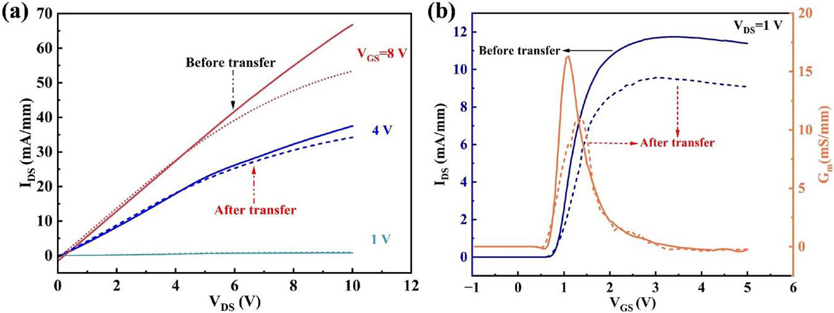
Figure 2: (a) Output and (b) transfer curves of AlGaN/GaN HEMT before and after the transfer.
The researchers blame self-heating effects for the lower drain current: “The sapphire temporary substrate has a significantly lower thermal conductivity (~30W/m-K) compared to the original silicon substrate (~150W/m-K), together with the 4μm-thick UV-curable adhesive layer, both of which are the primary cause of the exacerbated self-heating effect observed after transfer.”
The team suggests ways to mitigate the self-heating: “For practical flexible applications, heat dissipation can be engineered by thinning the flexible substrate to reduce thermal resistance, integrating high-thermal-conductivity fillers (e.g. BN or Al2O3) into the polymer, or using a thermally conductive adhesive interlayer.”
The researchers also compare the performance of their devices with other substrate release methods reported in the scientific literature (Table 1).
Table 1: Summary of performance variations of AlGaN/GaN HEMTs before and after transfer by various techniques.
Transfer method |
IDS,max reduction | Gm,max reduction |
| Electrochemical etching | 20.1% | 32.5% |
| Deep silicon etching | 34.0% | 29.2% |
| AlGaN/GaNOI undercut | 51.3% | 24.4% |
| Si undercut by wet etching | 36.5% | 24.5% |
| Si undercut by wet etching | 61.5% | 46.5% |
| Deep-reactive ion etch | 1.0% | 1.5% |
| Laser lift-off | 17.8% | 27.2% |
The team comments: “The extent of degradation observed in our work is comparable to that reported for other transfer methods, underscoring the viability of the present electrochemical lift-off approach.”
https://doi.org/10.1088/1361-6463/ae90bb
The author Mike Cooke is a freelance technology journalist who has worked in the semiconductor and advanced technology sectors since 1997.