

News: Optoelectronics
6 August 2026
More thermally stable indium phosphide quantum dot near-infrared laser diodes
Hong Kong University of Science and Technology (HKUST) in China reports multi-stack indium phosphide (InP) quantum dot (QD) 780nm lasers on silicon (Si) with a high characteristic temperature (T0) of 125K in the near infrared (NIR) [Wen Gu et al, Optics Letters, v51, p3641, 2026].
The devices benefited from optimizing the number of layers to 5, and by using silicon substrates rather than gallium arsenide (GaAs). In particular, the threshold current density was reduced through the improved modal gain from 5 layers of InP QDs, and the higher thermal conductivity of silicon resulted in better thermal management.
The team comments: “These results indicate that optimized active-region stacking is an effective approach to mitigate the thermal bottleneck of InP QD NIR lasers on silicon platforms.”
The researchers see monolithic integration of NIR InP QD lasers on silicon as being essential for on-chip quantum technologies and biophotonics, along with spectroscopy. However, up to now these devices have not been able to match the performance of the more mature communications wavelengths of 1.3μm and 1.5μm.
The team comments: “Achieving reliable NIR emission on silicon remains a challenge, as direct epitaxial growth of III-V materials on silicon is fundamentally hindered by lattice and thermal expansion mismatches. These mismatches induce high densities of threading dislocations, which act as non-radiative recombination centers that cause severe thermal quenching at elevated temperatures”
QD devices tend to be more tolerant of defects. For example, QDs have enabled 1.3μm lasers on silicon with T0 values of more than 200K.
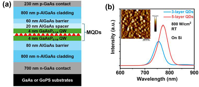
Figure 1: (a) Schematic of InP/GaAsP QD laser grown on GaAs or silicon substrates. (b) Room-temperature (RT) micro-photoluminescence spectra of the 3-layer and 5-layer QD structures on silicon. Inset: 1μm×1μm atomic force microscope (AFM) image of uncapped 5-layer QDs on silicon sample.
The material structures (Figure 1) were grown on GaAs substrates or GaAs on planar silicon (GoPS) templates by metal-organic chemical vapor deposition (MOCVD). The GoPS material was grown by MOCVD using a thermal cycle annealing and dislocation filter layers method developed at HKUST to reduce the defect density in the GaAs by a factor of 40. Relatively thick aluminium gallium arsenide (AlGaAs) cladding layers were used to ensure sufficient optical mode confinement.
The InP QD active regions were grown in GaAsP quantum wells (QWs), repeated 3 or 5 times, separated by AlGaAs spacers. The dots were grown at 680°C, while the rest of the structure was grown at 650°C. The 5-layer QD structure on silicon had a QD density of 1.8×10¹⁰/cm2.
The GaAsP QWs had a low phosphorus content, relative to previous HKUST QD structures. This reduced accumulated strain, allowing better quality multi-stacks of QDs.
The material was fabricated into ridge-waveguide laser diodes. The silicon substrate was thinned to enable cleaving into laser bars, and to reduce thermal resistance for better heat dissipation.
The devices were placed on a temperature-controlled copper stage, and operated in pulsed mode to avoid self-heating effects. The turn-on voltage was around 1.5V for all devices. The thicker 5-layer device on silicon had a slightly higher 13Ω on-resistance, compared with 9Ω for the 3-layer laser diode.
For ridges measuring 1.2mm×70μm, the laser threshold current density (Jth) was 0.94kA/cm2 for the 3-layer laser diode, and 0.86kA/cm2 for 5 layers.
The researchers comment: “The reduced Jth for 5-layer devices is due to the increase in their mode gain. In addition, 5-layer devices allow the threshold condition to be met at a lower carrier occupancy per dot. Consequently, this minimizes heat generation and suppresses carrier thermal escape into the barrier layers, enhancing thermal stability.”
The team also notes that there is a limit to adding layers, since the increased strain would eventually lead to material quality degradation.
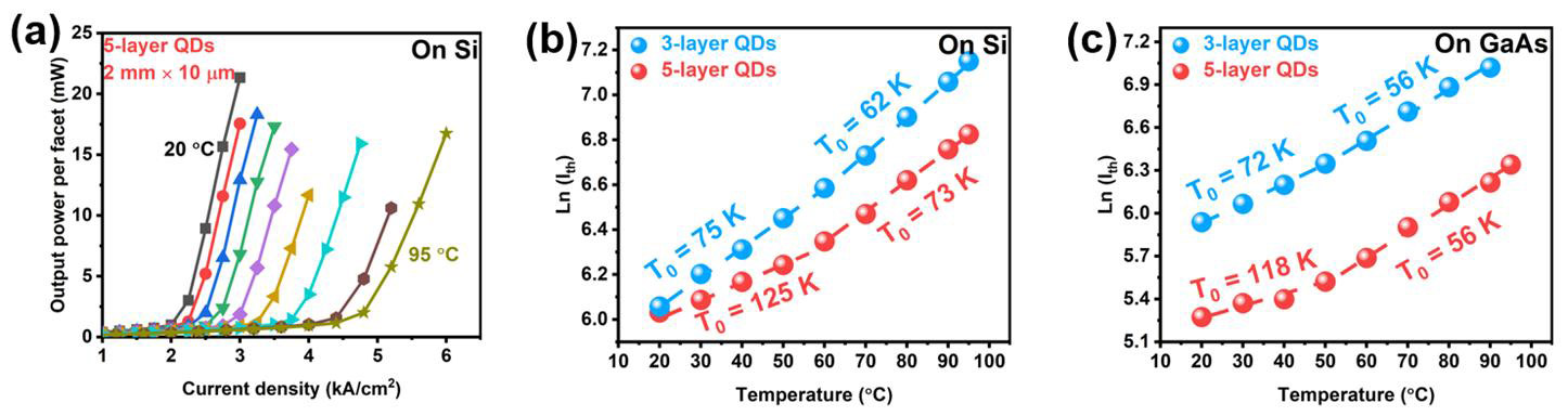
Figure 2: (a) Temperature-dependent light output power–current density characteristics from 20°C to 95°C for 5-layer QD laser on silicon (2mm×10μm). Comparison of extracted T0 of 3-layer and 5-layer QD lasers on (b) silicon and (c) GaAs substrates.
Studying the temperature dependence of the laser performance on temperature allowed extraction of the characteristic temperature (T0) for the threshold current increase (Figure 2).
The researchers report: “For the 5-layer QD laser on silicon, a high T0 of 125K was achieved in the 20–50°C range, representing a significant improvement over the 75K measured for the 3-layer counterpart on silicon. Above 50°C, both devices exhibit a typical reduction in T0 due to increased thermal carrier escape; however, the 5-layer QD laser on silicon maintains a higher T0 of 73K, outperforming the 62K of the 3-layer QD laser on silicon.”
The better T0 performance for the 5-layer device is attributed to increased modal gain from the extra layers. The devices on GaAs have somewhat lower T0 values due to the lower thermal conductivity of GaAs, relative to silicon.
The researchers compared their latest work with previous studies of similar devices emitting in the wavelength range 630–800nm (Table 1). The team sees their devices as being “highly competitive”.
Table 1: Comparison of T0 for MOCVD-grown InP QD lasers.
|
Wavelength (nm) | Stacking Number | T0 (K) | Substrate |
| Previous work: | ||||
| 757 | 5 | 74K (20–95°C) | Si | |
| 755 | 1 | 55K (20–60°C), 30K (60–95°C) | GaAs | |
| 638 | 1 | 124K (5–20°C), 49K (20–40°C) | GaAs | |
| 660 | 1 | 85K (5–25°C), 53K (5–55°C) | GaAs | |
| 741 | 5 | 52K (10–85°C) | GaAs | |
| 774 | 5 | 111K (7–47°C), 89K (47–87°C) | GaAs | |
| Latest HKUST work: | ||||
| 752 | 3 | 72K (20–50°C), 56K (50–90°C) | GaAs | |
| 771 | 5 | 118K (20–50°C), 56K (50–90°C) | GaAs | |
| 765 | 3 | 75K (20–50°C), 62K (50–95°C) | Si | |
| 780 | 5 | 125K (20–50°C), 73K (50–95°C) | Si |
“These findings confirm that increasing the stacking layers of the active region significantly enhances thermal stability and provides a robust solution for high-T0 light sources directly onto silicon platforms,” they write.
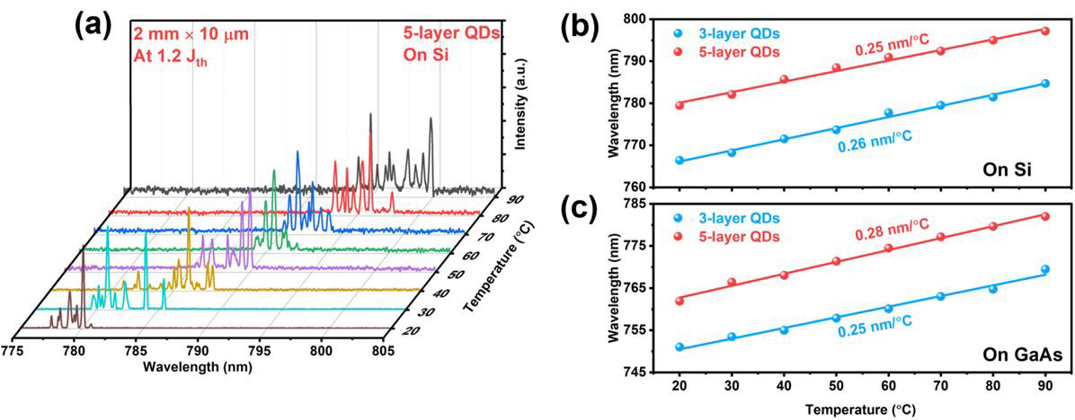
Figure 3: (a) Temperature-dependent lasing spectra of the 5-layer QD 2mm×10μm lasers at 1.2× threshold current. Temperature-dependent lasing peaks of 3-layer and 5-layer QD lasers on (b) silicon and (c) GaAs substrates.
The researchers also studied the spectral tuning capability with temperature (Figure 3). The team comments: “The similar thermal tuning behavior between the 5-layer QD laser on silicon and GaAs exhibits the high material quality of our monolithically integrated silicon-based light sources.”
InP quantum dot InP GaAs MOCVD
https://doi.org/10.1364/OL.604816
The author Mike Cooke is a freelance technology journalist who has worked in the semiconductor and advanced technology sectors since 1997.