

News: Microelectronics
4 August 2026
E-mode gallium nitride quantum well in aluminium nitride XHEMTs
Cornell University and Soctera Inc in the USA have reported enhancement-mode (E-mode) single-crystal (Xtal) high-electron-mobility transistors (XHEMTs) based on a coherently-strained gallium nitride (GaN) quantum well (QW)-channel layer between an aluminium nitride (AlN) barrier and substrate [Yu-Hsin Chen et al, Appl. Phys. Express, v19, p066501, 2026].
The researchers point out that the device structure could also be realized on silicon, silicon carbide (SiC) or sapphire substrates, expanding the possibilities for transfer to manufacturing.
The team adds: “Importantly, compared to conventional p-gated E-mode AlGaN/GaN HEMTs that require microns of GaN, here a few-nanometer-thick GaN quantum well is used, followed by shallow regrown source/drain GaN regions. This amounts to a dramatic reduction in gallium consumption for the device.”
The point here is that gallium is a relatively rare element, and hence expensive, in contrast to aluminium, which is widely available. The US geological survey reports world low-purity gallium production at 900 tonnes (900,000kg), compared with 74,000,000 tonnes for aluminium.
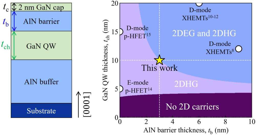
Figure 1: (a) AlN/GaN/AlN structure, with GaN cap. (b) AlN/GaN/AlN heterostructure phase diagram calculation with fixed 2nm GaN cap.
The GaN quantum well channel for the E-mode XHEMT was designed using an analytical model developed at Cornell (Figure 1). With a QW less than 20nm, the GaN can be grown coherently strained with the underlying AlN crystal. The strain-dependent charge polarization properties of the respective materials leads to the formation of effectively two-dimensional layers of electron and hole gases (2DEG/2DHG) in the GaN QW near the top and bottom interfaces, respectively. The respective carrier concentrations depend on the layer thicknesses. The Cornell researchers considered a sheet carrier density of 1012/cm2 as the phase boundary for the presence of 2DEG and/or 2DHG.
Researchers using the AlN/GaN/AlN structure have previously demonstrated n-channel XHEMTs and p-channel heterostructure field-effect transistors (HFETs) on bulk AlN with coherently strained GaN channels (circles in Figure 1). While the p-channel devices could operate in both depletion-mode (D-mode) and enhancement-mode (E-mode), the previous n-channel XHEMTs were D-mode. D-mode devices are normally on with 0 gate potential, while E-mode transistor operation is normally off. For many applications, the normally-off behavior is preferred for lower power consumption and fail safety, particularly for power systems.
The AlN/GaN/AlN material for the Cornell XHEMT (Figure 2) was grown by plasma-enhanced molecular beam epitaxy(MBE) on bulk AlN substrate. A GaN cap was added to protect the AlN from oxidation. The barrier and QW thickness were designed to be on or near the border between 2DHG and the 2DEG/2DHG regions to give the normally-off/E-mode behavior.
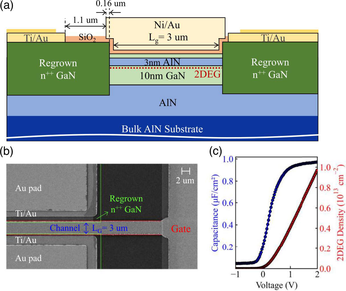
Figure 2: (a) Schematic cross section of the fabricated long-channel MOSFET. (b) Top-view scanning electron microscopy (SEM) image of fabricated device. (c) Capacitance−voltage measurements at room temperature using 5MHz excitation with 10μm gate length (LG) and 50μm width indicating n-type electron channel for positive voltages.
The source/drain contacts used MBE-regrown heavily n++-doped GaN in regions recessed by inductively coupled plasma etching. This ensured that current flowed predominantly through the 2DEG rather than the 2DHG when a suitable potential was applied to the gate.
The team comments: “An attractive feature in this structure is the regrowth of p-type GaN regions can create p-channel transistors on the same heterostructure. When combined with the E-mode n-channel transistor shown here, this presents a new approach to realize planar CMOS operation in wide-bandgap nitride semiconductors.”
The researchers likened the fabrication strategy to that used in mainstream silicon MOSFETs where heavily doped source/drain regions are formed using ion implantation, resulting in combinations of p-channel and n-channel transistors enabling complementary metal-oxide-semiconductor (CMOS) circuit designs.
The gate stack consisted of atomic layer deposition (ALD) silicon dioxide (SiO2) insulation and nickel/gold metal. The gate overlapped the regrown GaN regions, “similar to the device geometry of a planar silicon n-MOSFET,” the team comments. The source/drain metals were titanium/gold.
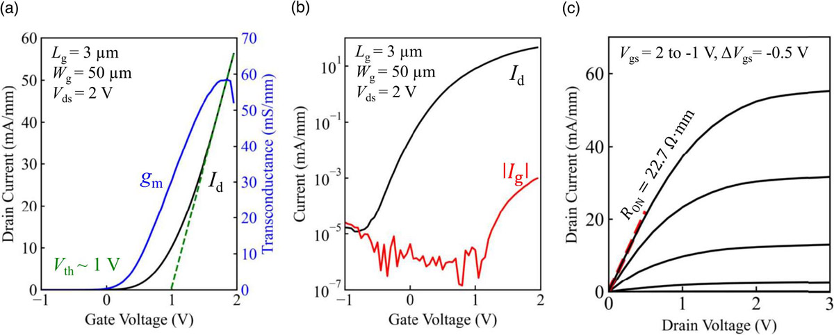
Figure 3: (a) Linear- and (b) logarithmic-scale transfer characteristics. (c) Output characteristics.
The E-mode XHEMTs with 3μm gate had a linear-extrapolation threshold of 0.99V (Figure 3). The researchers point out that, while linear-extrapolation values are relevant for amplifiers, they do not give an appropriate determination of the turn-on voltage for power switches. For example, a 1mA/mm off-state current determination would correspond to a slightly negative threshold voltage.
The team comments: “The drain current on the order of 10−2mA/mm at Vgs = 0V likely flows between the n+-GaN source and drain contacts via the low-density 2DEG channel with a sheet resistance on the order of MΩ/□.”
In other news, the on/off current ratio spanned six orders of magnitude. The drain current Id reached a maximum of 55.2mA/mm with 22.7Ω-mm on-resistance RON at 2V gate potential (Vgs). The sub-threshold slope was 166mV/decade at −0.35V gate and 2V drain (Vds). The maximum transconductance (gm) was 58.5mS/mm.
The researchers comment: “The very small gate–drain spacing, and the thin SiO2 in this first-generation device limit the maximum drain voltage that can be applied.”
They add: “Though E-mode XHEMTs are successfully designed and demonstrated for the AlN/GaN/AlN double heterostructure in this study, the device performance is limited and well below state of the art E-mode GaN HEMTs.”
The team suggests a number of potential enhancements:
(a) varying the GaN/AlN/GaN/AlN layer thickness to explore the design phase space in Figure 1, along with channel, barrier, and/or cap doping;
(b) different gate dielectrics and metal;
(c) gate length scaling.
Aluminium nitride XHEMTs XHEMTs GaN AlN SiC MBE
https://doi.org/10.35848/1882-0786/ae6a5b
The author Mike Cooke is a freelance technology journalist who has worked in the semiconductor and advanced technology sectors since 1997.