


News: Microelectronics
11 September 2025
Boron nitride as a buffer and gate dielectric
Xidian University in China has reported the use of ultrawide-bandgap hexagonal boron nitride (hBN) to improve the performance of aluminium gallium nitride (AlGaN) high-electron-mobility transistors (HEMTs) [Haoran Zhang et al, IEEE Electron Device Letters, published online 19 August 2025]. The BN was used both as a buffer for van der Waals epitaxy, and as part of the gate stack. These features enabled an extremely high ~1011 on/off current ratio, along with a high maximum saturated output current density of 1550mA/mm.
Boron nitride is a two-dimensional (2D) material consisting of hexagonal layers, like graphene, held together by weak van der Waals interlayer bonds. The Xidian team comments: “Recent GaN synthesis using a 2D material technology has attracted considerable research interest. The weak bonding between 2D materials and GaN effectively reduces stress caused by lattice mismatches during heteroepitaxy, thereby greatly decreasing the dislocation density and improving the material quality.”
The researchers see potential for application in high-power electronic systems.
The epitaxial material for the HEMTs was produced on sapphire with and without a BN buffer layer (Figure 1). The BN was grown on copper (Cu) foil via chemical vapor deposition (CVD) and transferred by transparent poly(methyl methacrylate) (PMMA) thermoplastic onto the sapphire substrate covered with 30nm sputtered AlN layer.
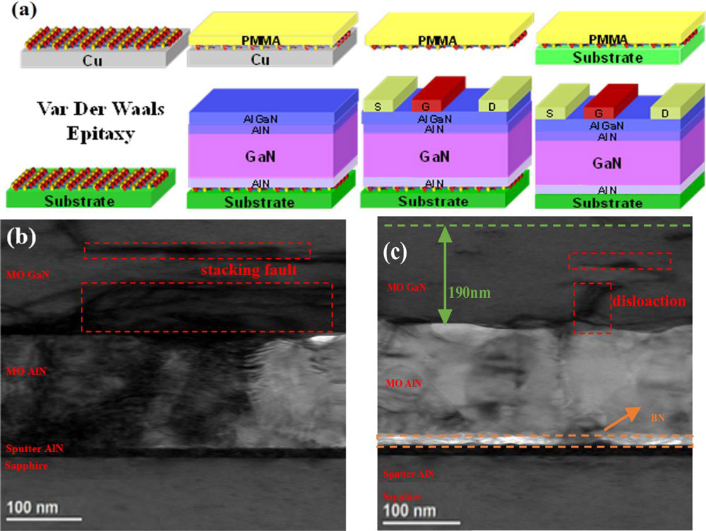
Figure 1: (a) Van der Waals epitaxy process and cross-sectional schematics of AlGaN/GaN HEMTs. (b) Interface scanning transmission electron microscope (STEM) cross section of bottom layer of sample without BN buffer. (c) Same but with BN buffer.
The researchers report: “The inclusion of the hBN buffer significantly enhances device performance. Compared to the samples without hBN buffer, the introduction of the hBN buffer layer increases the 2DEG sheet density from 5.8x10¹²/cm2 to 1.24x10¹³/cm2, enhances the electron mobility from 1726cm2/V-s to 2091cm2/V-s, and reduces the sheet resistance (Rsh) from 430Ω/□ to 290Ω/□.”
The team attributes these improvements to the transport properties of the 2D electron gas (2DEG) channel to “dislocation filtering and crystal quality enhancement” from using the BN buffer layer. The rest of the device material consisted of 200nm AlN, 1.2μm GaN buffer, 300nm undoped GaN, and 25nm Al0.25Ga0.75N barrier, applied using metal-organic CVD.
A low-cost 8nm sputtered BN layer was added as a gate dielectric, after removing the GaN cap layer used to protect the AlGaN barrier from contamination such as oxidation. This dielectric thickness was chosen on the basis of simulations suggesting that the on/off current ratio would have a maximum at 7nm. The choice of 8nm took account of the deposition method and the minimal deterioration of the on/off ratio beyond 7nm in the simulations. The magnetron sputtering source was BN. The samples were annealed beforehand.
Four types of HEMT were fabricated exhausting the possible combinations with and without BN used for the buffer and gate dielectric. The gate length and gate−source/−drain spacings were 150nm and 850nm/1μm, respectively. The gate width was 50μm.
The HEMT with both BN buffer and dielectric (sample A) outperformed the other variations (Figure 2). In particular, the on/off ratio was around 1011, some three orders of magnitude better than sample D with no BN at all. The other variations, B and C, had BN only as the buffer and dielectric, respectively.
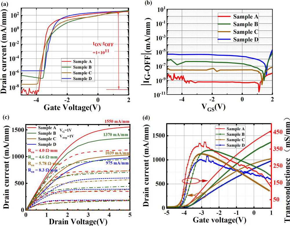
Figure 2: (a) Device-transfer semi-logarithmic curves. (b) Device leakage curve. (c) Output current−voltage characteristics. (d) Transfer characteristics.
The devices with BN dielectric exhibited a more negative threshold (around −0.5V), attributed to “positive fixed charges at the BN dielectric/AlGaN interface, resulting in a downward shift of the flat-band voltage (VFB) and a more negative threshold voltage (Vth).” Since all the devices are ‘normally-on’ at 0V gate potential, this is undesired behavior in many power applications, where normally-off (enhancement mode) devices offer benefits in terms of lower power consumption, fail safety, and so on.
The maximum saturated output current densities for HEMTs A–D were 1550mA/mm, 1370mA/mm, 1039mA/mm and 975mA/mm, respectively.
The researchers comment: “The increase in the maximum saturated output current density may be related to the improved crystal quality, lower dislocation density, and enhanced 2DEG achieved by the introduction of the h-BN buffer. Additionally, the introduction of the BN gate dielectric further improves the interface quality, reduces the surface state density (Dit), and minimizes interface charge, thereby enhancing the gate’s control over the channel carriers, improving carrier transport, and ultimately improving the conductivity of the device.”
The peak transconductance of HEMT-A was 30% higher than that of D: 360mS/mm compared with 251mS/mm at 5V drain bias. The more significant contributor to improved transconductance was the BN buffer, giving improved conductivity in the channel.
In pulse-mode operation, HEMT-A demonstrated a current collapse of 6%. “The BN/AlGaN interface effectively suppresses trap-assisted carrier scattering and mitigates dynamic degradation by reducing trap occupancy modulation during switching,” the team comments. Current collapse in conventional GaN HEMTs can be of order 30%.
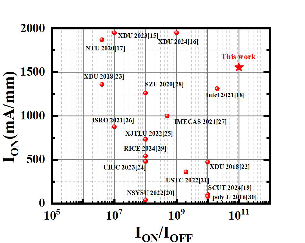
Figure 3: Benchmarking maximum saturated output current density and on/off current (I) ratio.
Comparing the Xidian work with other reports shows the highest on/off ratio combined with a good maximum saturated output current density (Figure 3).
https://doi.org/10.1109/LED.2025.3600447
The author Mike Cooke is a freelance technology journalist who has worked in the semiconductor and advanced technology sectors since 1997.


