


News: Suppliers
1 September 2025
University of Wisconsin-Madison opens Ultra-Wide Bandgap Semiconductor MOCVD Lab
The University of Wisconsin-Madison’s Engineering Centers Building on 5 August hosted the grand opening of the Ultra-Wide Bandgap Semiconductor Metal-Organic Chemical Vapor Deposition (MOCVD) Laboratory, attended by university and national R&D leaders including UW-Madison’s vice chancellor for research Dorota Grejner-Brzezinska; College of Engineering Dean Devesh Ranjan; and Vivek Prasad, VP for design engineering ecosystem enablement at NatCast (a nonprofit that operates the National Semiconductor Technology Center). They joined Susan Hagness, chair of the Department of Electrical and Computer Engineering and ECE assistant professor Shubhra Pasayat, who oversees the new facility as the lab’s principal investigator.
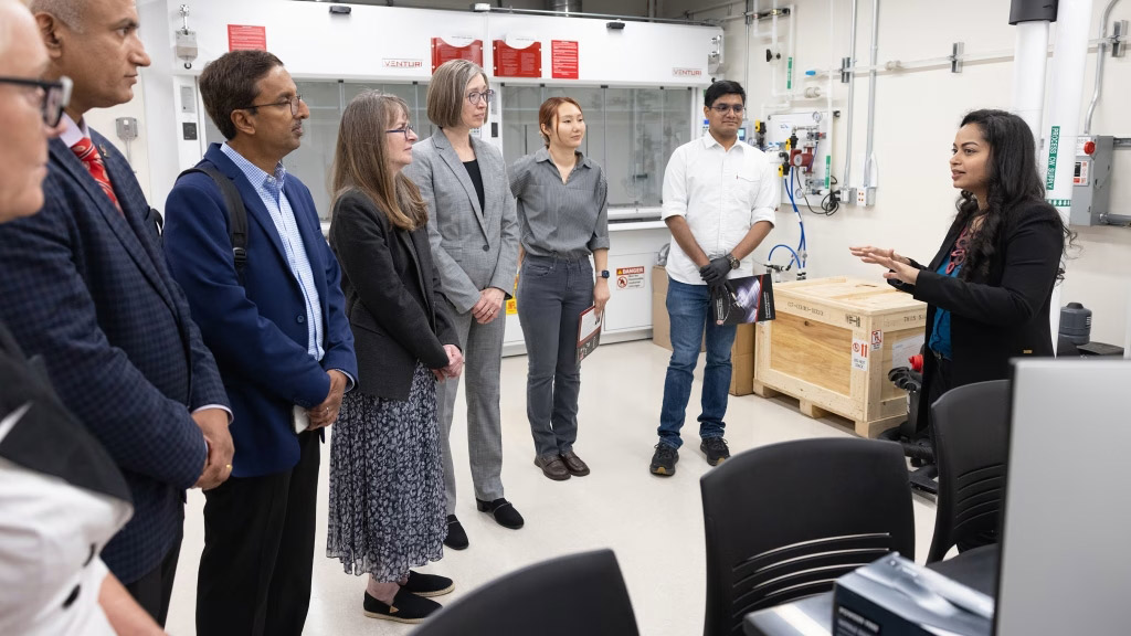
Picture: At the grand opening of the new lab, Shubhra Pasayat (right) gave tours to faculty and staff including (left to right) UW-Madison vice chancellor for research Dorota Grejner-Brzezinska; College of Engineering Dean Devesh Ranjan; Vivek Prasad, vice president for design engineering ecosystem enablement at NatCast; associate vice chancellor for research Amy Wendt; and ECE chair Susan Hagness. Photos: Todd Brown.
The facility will serve as the cornerstone of the College of Engineering-led focus at UW-Madison on III–nitride semiconductors. Pasayat cites applications including deep ultraviolet LEDs; high-power radar; high-voltage power electronics, motors, and vehicles; as well as nuclear reactors and applications in other extreme conditions like space.”
As they allow for smaller, faster, more efficient electronic devices that can handle much higher energies and frequencies, the electronics industry is already rapidly adopting wide-bandgap semiconductors such as silicon carbide (SiC) and gallium nitride (GaN) for use in fast chargers, radar systems, LED lighting and microchips. As fabrication techniques improve and costs decrease, wide-bandgap semiconductors are expected to become more commonplace.
But researchers are already looking past these wide-bandgap semiconductors to ultrawide-bandgap materials, including the III–nitride semiconductors aluminium gallium nitride and aluminum nitride, which are even more robust, and able to survive conditions ranging from the extreme temperatures found in hypersonic jets to radiation in modular nuclear reactors. They can also handle the wide frequency switching in 6G communications and beyond, among other emerging applications.
At the moment, fabricating and characterizing these ultrawide-bandgap semiconductors is challenging because they require expensive equipment and deep expertise in MOCVD or other advanced commercialization-friendly deposition techniques.
When she first joined UW-Madison in 2021, Pasayat set up a commercial Aixtron MOCVD reactor, which can grow wide-bandgap materials like gallium nitride and low-aluminium aluminum gallium nitride (AlGaN).
Now, the new facility — which took years of planning and cooperation among UW-Madison, the College of Engineering and the Department of Electrical and Computer Engineering — takes that research to the next level. The newly installed Agnitron Agilis 100 system can handle even higher temperatures and lower pressures, allowing Pasayat and her students to design and precisely synthesize high-quality 2-inch-diameter wafers of high-aluminium-content AlGaN, AlN and other ultrawide-bandgap materials.
Pasayat says this capability is already opening up a huge number of collaborations with researchers across campus and is drawing industry partners to UW-Madison. It is also an opportunity for students who will enter the workforce trained on some of the most advanced fabrication equipment available and with hands-on knowledge of next-generation materials, she adds.
Pasayat’s lab is at the center of UW-Madison’s III–nitride ecosystem. The onsite faculty’s broad expertise in chip design and architecture, materials characterization, fabrication, advanced packaging, and systems integration means that these ultrawide-bandgap semiconductors can go from the drawing board to the motherboard all on one campus — streamlining and improving the research process.


