


News: Optoelectronics
25 September 2025
MOCVD–MBE hybrid growth for green laser diodes
Researchers in China propose the use of hybrid growth methods for longer-wavelength indium gallium nitride (InGaN) laser diodes (LDs) [Jun Fang et al, Appl. Phys. Lett., v127, p072105 2025].
The main methods for growing high-quality III–nitride crystal device layers such as InGaN are metal-organic chemical vapor deposition (MOCVD) and molecular beam epitaxy (MBE). While MOCVD is favored in terms of growth speed, the slower MBE method is usually carried out at lower temperature.
High-temperature growth can degrade previous layers. This is particularly critical for the high-indium-content InGaN needed in the multiple quantum well (MQW) structures of longer-wavelength-emitting laser diodes. Indium is much more volatile than the other metals in the III–nitride family, such as gallium and aluminium (Al). Indeed, due to this volatility, InGaN MOCVD is usually carried out around 700°C to avoid degradation.
But, in subsequent AlGaN cladding layers, MOCVD temperatures are raised to 950–1050°C to achieve the quality needed for optical confinement, gobbling up the thermal processing budget.
MBE processing can achieve decent AlGaN quality with lower temperatures of order 700–750°C, easing the budget constraints.
The research team from University of Science and Technology of China, Suzhou Institute of Nano-Tech and Nano-Bionics, and Suzhou Laboratory in China comments: “The growth of p-type (Al)GaN under low-temperature conditions using MBE is expected to further extend the wavelength range of GaN-based lasers.”
The lower layers of the laser diodes were grown by MOCVD on GaN substrates (Figure 1). For the ‘A’ laser diodes, the MOCVD continued, while for ‘B’ the epitaxy was switched to the lower-temperature MBE method, for the upper cladding and contact layers. The upper-cladding MOCVD temperature was around 900°C; the use of MBE allowed the growth temperature to be reduced to 700°C.
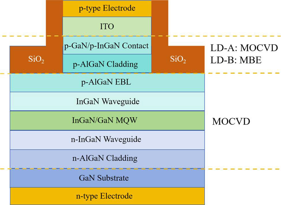
Figure 1: Schematic structure of GaN-based green laser diode. Sample LD-A was grown entirely by MOCVD, while sample LD-B was epitaxially deposited using the hybrid MOCVD–MBE growth approach.
These epitaxial materials were fabricated into ridge laser diodes with 200nm inductively coupled plasma CVD silicon dioxide (SiO2) insulation, 200nm electron-beam-evaporated indium tin oxide (ITO) contact layer and palladium/platinum/gold p-electrode. The n-electrode on the backside of the device was titanium/aluminium/titanium/gold. The emission/mirror facets were cleaved with optical dielectric coatings applied to improve performance.
Large samples of devices from various locations on the source wafers were characterized in terms of threshold current density, laser wavelength, slope efficiency and output power (Figure 2). The spread in numbers, as indicated by the standard deviation, was significantly smaller in the LD-B sampling for all parameters.
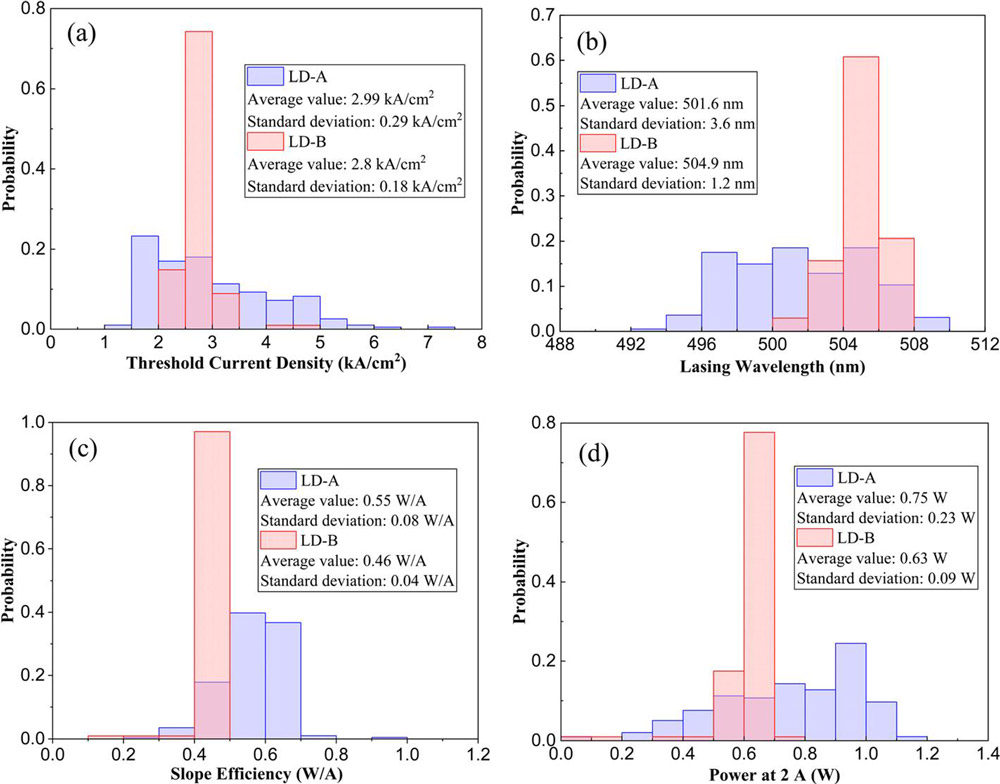
Figure 2: Histograms of (a) threshold current density, (b) lasing wavelength, (c) slope efficiency, and (d) output power at 2A current for LD-A and LD-B chips.
The researchers comment: “In terms of the best-performing individual chips, LD-A exhibits a lower threshold current density. However, the average threshold current density of LD-A is substantially higher based on the overall statistical results. This observation may be attributed to two underlying physical mechanisms: (1) increased non-radiative recombination centers — LD-A’s QWs have suffered more severe thermal degradation, leading to a greater density of non-radiative centers, which reduce carrier radiative recombination efficiency and consequently increase the threshold current density; (2) increased optical loss — the thermal degradation can roughen quantum well interfaces and increase the defect density, thereby increasing the internal optical loss. Greater optical loss results in higher threshold current density.”
The lasing wavelength of the LD-A devices was generally shorter wavelength, attributed to variable thermal degradation of the InGaN multiple quantum wells during the high-temperature MOCVD. Degradation effects include phase separation of regions of lower and higher indium content, along with reduced indium content overall. Lower-indium-content InGaN has a wider bandgap energy, resulting in higher-energy, shorter-wavelength photons.
The lower average slope efficiency of LD-B is attributed to the higher magnesium doping of the upper cladding layers. High Mg-doping has been found to result in high optical absorption, significantly reducing slope efficiency in green InGaN laser diodes. The optical absorption has to be balanced by the need to reduce series resistance, the purpose of doping after all, between the external bias and the MQW region.
InGaN GaN substrates LDs MOCVD MBE
https://doi.org/10.1063/5.0289525
The author Mike Cooke is a freelance technology journalist who has worked in the semiconductor and advanced technology sectors since 1997.


