


News: LEDs
4 September 2025
Laser transfer of blue micro-LED arrays
Shanghai University and Shanghai Key Laboratory of Chips and Systems for Intelligent Connected Vehicle in China have reported on a direct laser transfer process of blue gallium nitride (GaN) micro-LED arrays to a silicon substrate using rubber tape [Zhu Yang et al, Appl. Phys. Lett., v127, p051104 2025].
Micro-LEDs produced in the indium gallium nitride (InGaN) semiconductor family are being widely developed for high-resolution, high-brightness, and high-energy-efficiency application in fields such as augmented reality/virtual reality (AR/VR), wearable devices, and automotive displays.
The researchers comment: “In the micro-LED display manufacturing route, monolithic integration technology is suitable for small-size, high-resolution micro-displays, but there are still problems such as high difficulty in colorization, high cost of CMOS driver, and difficulty in repairing non-bright pixels. However, the mass transfer technology can more conveniently solve the above-mentioned problems and is suitable for the manufacturing of large-sized displays. It has become a technical bottleneck restricting the mass production of micro-LED large-sized display devices.”
The material for the micro-LEDs was grown by metal-organic chemical vapor deposition (MOCVD) on 4-inch sapphire (Figure 1). The fabricated LEDs included a magnetron sputtering indium tin oxide (ITO) layer on the p-GaN contact for current spreading. Plasma-enhanced CVD (PECVD) silicon dioxide provided 200nm-thick electrical isolation. The metal electrodes were chromium/platinum/gold. The micro-LEDs measured 15μmx30μm in an array at x, y pitch of 40μm and 120μm, respectively.
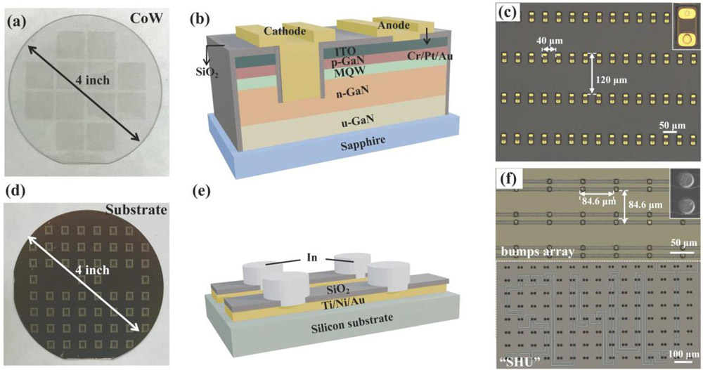
Figure 1: Diagrams of (a) chip-on-wafer (CoW) micro-LED source and (d) target substrate. (b) Micro-LED structure and (e) indium bumps on silicon substrate. Optical images of (c) micro-LED array on sapphire, and (f) indium bump array on silicon, substrates.
The target substrate for the micro-LED array was 4-inch silicon with patterned titanium/nickel/gold, covered by 200nm PECVD silicon dioxide. Indium (In) bumps were deposited as 8μm positive and negative contacts were separated by 20μm. The 30x15 bump array spacing was 84.6μm.
The researchers worked with German company TESA to develop the rubber tape used for transferring the micro-LEDs to the target substrate (Figure 2). The desired properties of the tape included ease of die cutting, compatibility with various carrier sizes, superior chip retention, and solvent washability.
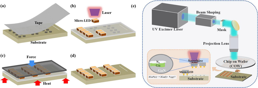
Figure 2: Process scheme: (a) attach rubber tape, (b) laser transfer, (c) thermo-compression bonding, and (d) tape removal. (e) Laser transfer system separating GaN LEDs from sapphire substrate.
The micro-LED dies were separated from the growth substrate by decomposing the interface between the GaN buffer and sapphire substrate by 20ns pulsed 248nm ultraviolet (UV) excimer laser light. The wavelength gave photons with energies above the bandgap of the GaN buffer, but below that of the sapphire substrate. The light was therefore absorbed by the GaN, but not the sapphire.
The researchers explain: “This results in a rapid temperature increase at the GaN–sapphire interface, causing GaN decomposition into liquid gallium (Ga) and nitrogen gas (N2). Consequently, this decomposition facilitates the detachment of GaN micro-LEDs from the sapphire substrate and their seamless transfer to the target substrate.”
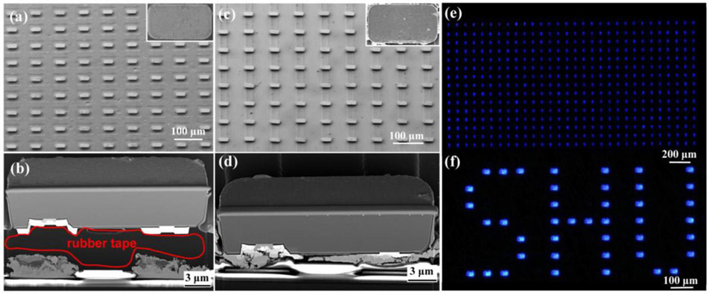
Figure 3: SEM images of micro-LED array after transfer (a), and single micro-LED cross section sliced by focused ion-beam (FIB) (b); images of array and single micro-LED cross section after bonding (c) and removing substrate tape (d); (e) EL images of 30x15 micro-LED display and (f) with “SHU” abbreviation commonly used for Shanghai University.
The micro-LEDs were transferred on the rubber tape to the target and bonded by a thermo-compressive force of 5kg weight at 160°C for 5 minutes with the tape between the flipped chip array and the target substrate (Figure 3). After attachment, the micro-LEDs were cleaned with ethyl acetate, removing the tape and other residues.
The researchers report: “the micro-LED array exhibits no flipping or off-setting, with electrodes precisely embedded in the rubber tape and positioned above the bumps.”
Scanning electron microscope (SEM) images taken after bonding and removal of the tape showed no chip detachment with the electrodes connected to the indium bumps. “However, minute cracks are visible at the bonding interface,” the team adds.
Current-voltage tests of the devices showed “no significant difference between before and after transfer”. The team comments that a slight operating voltage increase “may be due to the stress release in the micro-LED after transfer, which attenuates the quantum-confinement Stark effect (QCSE) and improves the radiative compounding efficiency, thus compensating for the increase in the operating voltage.”
The brightness of the LEDs was reduced after transfer, “but still remains at the same order of magnitude”. The team reports: “At 1mA, the average brightness is 1.17x10⁶cd/m2 and 1.03x10⁶cd/m2 before and after transfer, respectively, indicating a 12.3% reduction.”
The transfer process also introduced a slight blue-shift: “The peak wavelength shifted from 454.1nm to 449.4nm at 30μA and from 444.2nm to 443.0nm at 1mA, respectively. This shift can be attributed to stress relief in the epitaxial layer after transfer, weakening the QCSE and widening the bandgap. Additionally, laser-induced defects in the GaN thin-film lattice during transfer may contribute to wavelength variations.”
The width of the peak was also reduced by transfer. The array was also subjected to shear tests, demonstrating an average 64.67MPa. This is described as comparable to other reports of Au-In bonding in flip-chip micro-LEDs subjected to thermo-compression at 160°C under 5kg force.
GaN GaN micro-LED arrays Silicon substrate MOCVD PECVD
https://doi.org/10.1063/5.0272689
The author Mike Cooke is a freelance technology journalist who has worked in the semiconductor and advanced technology sectors since 1997.


