


News: Microelectronics
1 September 2025
Nagoya University produces gallium oxide pn diodes with double current-handling capacity
Gallium oxide (Ga2O3) can make electronic devices much more energy efficient than existing silicon-based technology. For electronic diodes, researchers have been able to reliably produce n-type gallium oxide layers but struggled to create stable p-type layers because gallium oxide's crystal structure naturally resists the atoms needed for these layers. This limitation resulted in gallium oxide semiconductors with poor performance and reliability issues.
Now, researchers at Japan’s Nagoya University claim to have solved this manufacturing challenge and created the first functional pn diodes using gallium oxide (Naohiro Shimizu et al, ‘p-type layer formation study for Ga2O3 by employing Ni ion implantation with two-step oxygen plasma and thermal annealing’, Journal of Applied Physics (2025), 138(6). DOI: 10.1063/5.0282789). Their method enables the use of gallium oxide for improved semiconductors and energy-efficient devices. In addition, the new pn diodes can carry twice as much electrical current as previous gallium oxide diodes.
Quest to produce a stable p-type gallium oxide layer
Existing silicon-based pn diodes can handle high voltages but waste a lot of energy as heat, especially in energy-intensive applications such as electric vehicles and renewable energy power grids.
Gallium oxide pn diodes can handle twice the current capacity of previous gallium oxide devices and waste less energy than silicon-based diodes, notes Nagoya. This makes them suitable for demanding applications and translates to decreased cooling requirements, better energy efficiency in high-power systems, and lower operating costs.
The problem was that gallium oxide’s crystal structure easily accepts the atoms needed to create n-type layers but rejects the atoms required for p-type layers. Previous methods to force them in either failed or required temperatures that destroyed the material. Without both types working together, gallium oxide remained limited for practical applications.
To address this, the researchers implanted nickel atoms into the gallium oxide layer. They then heated the material twice, first at 300°C with activated oxygen radicals (given extra energy using proprietary plasma treatment) and then at 950°C in oxygen gas. This converted the embedded nickel into nickel oxide and properly integrated it with the gallium oxide crystal structure.
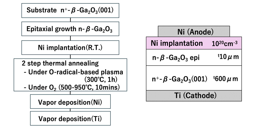
Graphic: Illustration of the new fabrication process: ion implantation of nickel atoms, followed by low-temperature plasma treatment and high-temperature annealing to create stable p-type layers in gallium oxide. Credit: Center for Low-Temperature Plasma Sciences, Nagoya University.
Future impact and innovation
“Since this method uses standard industrial equipment and processes, it can be scaled up for mass production,” notes professor Masaru Hori at the Center for Low-Temperature Plasma Sciences at Nagoya University. “The implications for future energy efficiency and costs are substantial, particularly for electric vehicle and renewable energy industries.”
The gallium oxide semiconductor market is projected to reach 14.9bn yen annually by 2035. This new manufacturing process is reckoned to solve a fundamental problem that previously limited industrial applications. Nagoya University spin-off company NU-Rei is now working to bring these advances to market.


