


News: Suppliers
3 September 2025
Nagoya spinoff Photo electron Soul’s GaN-based e-beam technology targets semiconductor inspection & metrology
In late September, Japan-based KIOXIA Iwate Corp will begin evaluating a gallium nitride (GaN)-based electron-beam technology developed through joint research between Nagoya University spinoff Photo electron Soul Inc (PeS) and the Amano–Honda Laboratory at Nagoya University.
PeS has developed an electron gun specialized for GaN photocathodes and has demonstrated its effectiveness for semiconductor inspection and metrology (I&M), enabling electron microscopy of nanoscale transistors and high-aspect-ratio structures.
The advance is said to open up possibilities for non-contact electrical I&M during the front-end stages of semiconductor manufacturing — previously unattainable with conventional technologies — as well as defect and structural I&M deep inside high-aspect-ratio features, both of which could improve semiconductor manufacturing yield.
KIOXIA Iwate will begin evaluating the technology in its production lines to verify its impact on defect detection, yield improvement, and root-cause analysis.
GaN photocathodes achieve industrial breakthrough
The potential value of photoelectron beam technology from semiconductor photocathodes for semiconductor manufacturing I&M has been recognized for more than a quarter of a century, yet its industrial application has been limited by issues of fragility. To overcome this, Nagoya University has developed GaN photocathodes, achieving more than 20-fold improvement in durability over conventional technologies and realizing a breakthrough toward electron-beam innovation that had been sought for nearly five decades.
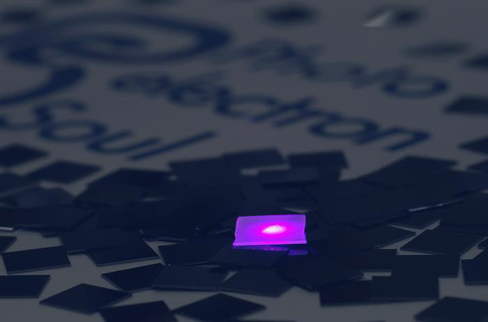
Picture: At the center, the violet glow of a GaN photocathode, surrounded by silicon crystals. (Photo courtesy of Photo electron Soul Inc.)
Further advances were achieved by PeS, which developed a type of electron gun specialized for GaN photocathodes. This demonstrated the lifetimes and uptime stability necessary for the semiconductor manufacturing environment, reinforcing the industrial viability of GaN photocathodes. Moreover, PeS has focused on pulsed e-beams and invented Digital Selective e-Beaming (DSeB), a technique that synchronizes e-beam scanning in scanning electron microscopy (SEM) with the laser irradiating the photocathode. This enables the delivery of e-beams with controlled intensity to arbitrary pixel-level locations within SEM images, opening up new possibilities for selective e-beam irradiation in semiconductor I&M.
Innovative approach to semiconductor inspection and metrology
While process technologies for device miniaturization and 3D integration are well established, I&M technologies began to reach critical limitations without any solutions in sight for solving yield issues, says KIOXIA Iwate. However, PeS has demonstrated the effectiveness of a new I&M approach that addresses the following two challenges in semiconductor manufacturing:
- Electrical I&M of nanoscale transistors
In chips consisting of densely integrated nanoscale transistors, it is extremely difficult to perform electrical testing of individual transistors by conventional contact probing. Using DSeB, specific regions of nanoscale transistors within memory devices were selectively irradiated with the e-beam. By exploiting electron-beam-induced charging to generate gate bias (non-contact switching), PeS observed this electrical behavior in SEM images. - I&M of 3D semiconductor devices with high aspect ratios:
In advanced devices such as 2.5D and 3D chiplets, high-aspect-ratio trench structures with submicron openings are introduced. This makes it challenging to inspect and measure sidewalls, bottom structures, and defects. For deep observation of high-aspect-ratio silicon trenches, DSeB was used to selectively target the trench bottoms, enabling the detection of residues and visualization of bottom structures.
These achievements open up new possibilities not only for non-contact electrical I&M during the front-end stages of semiconductor manufacturing — previously unattainable with conventional technologies — but also for defect and structural I&M in deep high-aspect-ratio regions. Accordingly, this project is expected to provide a novel solution to persistent yield challenges in semiconductor device fabrication.
Significance and outlook
Based on these demonstrations, KIOXIA Iwate will begin evaluating the technology in its production lines with the goal of making it a core technology for future semiconductor manufacturing. The firm will conduct detailed evaluations in actual production processes to determine its impact on yield improvement through enhanced defect detection and root-cause analysis.


