


News: Optoelectronics
2 October 2025
Quantum cascade lasers on a mid-infrared silicon photonic platform
Université Grenoble Alpes and Université Claude Bernard Lyon 1 in France have reported progress on integrating mid-infrared (MIR) III-V quantum cascade laser (QCL) diodes on a silicon photonics platform through molecular bonding [Maxime Lepage et al, Optics Express,v33, p37614, 2025].
The researchers comment: “Stable pulsed operation was maintained up to 72°C, with a characteristic temperature T0 of 180K, comparable to state-of-the-art QCLs on native III-V substrates.”
The researchers see opportunities for environmental monitoring, medical diagnostics, and industrial sensing, based on MIR spectroscopy. “A fully integrated MIR silicon photonic chip would enable cost-effective mass production using CMOS-compatible fabrication, paving the way for consumer-grade MIR devices and large-scale onsite sensing applications,” they write.
However, in this wavelength range the optical coupling between III-V and silicon is particularly challenging. To improve the coupling performance, the team adopted what they believe to be a novel approach, using high-index-contrast, phase-matched silicon on nitride on insulator (SONOI) substrate for the silicon photonic integration with the QCL through molecular bonding.
“The successful implementation of adiabatic coupling through a phase-matched high-index-contrast platform not only addresses a long-standing limitation in III-V/Si hybrid integration but also sets the stage for the co-integration of additional passive and active MIR components,” the researchers report, adding “Continuous-wave operation, the integration of on-chip detectors, and the extension toward dual-comb spectroscopy are promising avenues that could turn this platform into a fully functional MIR lab-on-a-chip.”
The researchers designed the integration so that the III-V provided optical gain, while feedback, coupling, and power extraction were provided by the phase-matched, high-index-contrast SONOI photonic integrated circuit (PIC) platform (Figure 1). The optical field was confined in a series of InGaAs/InAlAs multiple-quantum wells (MQWs) in a quantum cascade structure with peak gain around 4.31μm wavelength. The target dimensions of the III-V waveguide were 2mmx10μmx5.2μm.
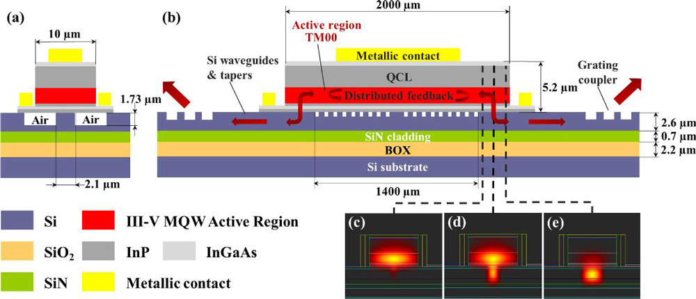
Figure 1: Transversal (a) and longitudinal (b) schematic views of laser. (c–e) Distribution of TM00 optical mode along taper transition: (c) taper input, (d) taper midpoint, (e) taper output.
The PIC structures used a 700nm silicon nitride (SiN) cladding layer to isolate the optical field from the buried oxide (BOX) layer. The QCL distributed feedback was provided by a quarter-wave shifted grating etched into the underlying silicon waveguide with 870nm slab and 1.73μm rib heights.
The optical coupling between the III-V gain medium and silicon waveguide PIC had a theoretical coupling efficiency exceeding 95% through tapering from 2.1μm to 4μm width over a 290μm transition region. External power extraction at a 20° angle to the surface normal was through grating couplers leading to an indium fluoride mid-IR optical fiber.
The researchers used finite-element and finite-difference optical simulations to optimize the designed structures.
The SONOI substrate was based on a 200mm-diameter silicon-on-insulator substrate with Si and SiN chemical vapor deposition layers transferred onto an oxidized silicon substrate. Mechanical grinding and selective chemical etch resulted in the final SONOI substrate.
The III-V heterostructure was grown on a 3-inch indium phosphide (InP) substrate. The material was bonded to the SONOI using oxygen plasma activation of the native oxide surfaces of the III-V material and the PIC substrate.
The researchers comment: “This plasma activation increases the density of surface hydroxyl (-OH) groups, enabling the formation of covalent molecular bonds at the interface. Once plasma-activated, both surfaces are brought into contact at room temperature to initiate the bonding. To further consolidate the bonding interface, a 2-hour annealing at 300°C is performed.”
The silicon surface of the substrate was meshed with vertical out-gassing channels to prevent voids forming from released gases such as hydrogen and steam during annealing of the molecular bonds between the III-V flipped onto the SONOI substrate.
The laser structure with metal contact was fabricated after removal of the InP substrate and etch stop layers (Figure 2).
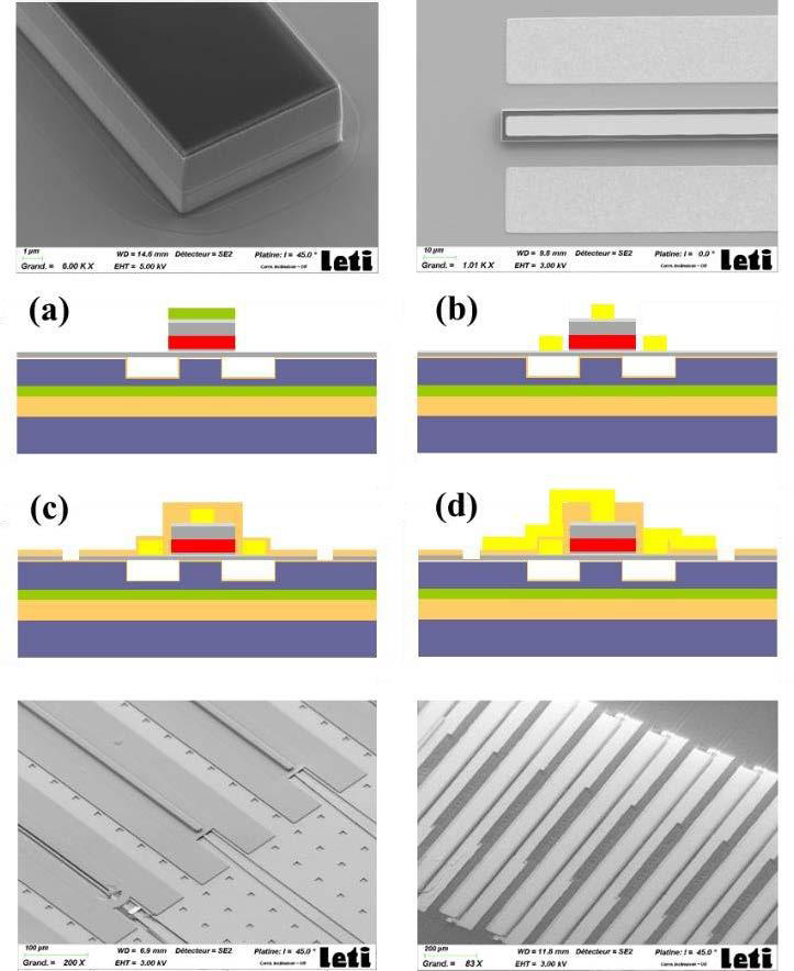
Figure 2: Process flow for III-V patterning and formation of electrical contacts. (a) Dry etching of top InP cladding and active region. (b) Metallic contact deposition and patterning via lift-off. (c) Passivation and etching of bottom III-V layers. (d) Opening of passivation layer followed by deposition and patterning of contact pads.
The threshold current and voltage of a typical device in 12°C pulsed operation were 3.5kA/cm2 and 16V, respectively. Single-mode emission up to 4kA/cm2 was observed at 4.315μm wavelength, consistent with the design parameters. Multi-mode emissions continue until output power rollover at 340μW, around 5.5kA/cm2. Accounting for fiber propagation losses and grating extraction efficiency, the team estimates a maximum on-chip power of more than 476μW.
The QCL assembly was also operated at different temperatures up to 72°C (Figure 3). The expected exponential evolution of the threshold with temperature showed an extracted characteristic temperature T0 of 180K, “a value consistent with those reported for low-doped quantum cascade lasers fabricated on native InP substrates and operating under pulsed, low-duty-cycle conditions,” according to the team.
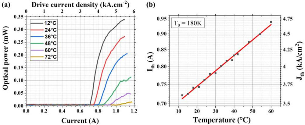
Figure 3: (a) Temperature-dependent optical power, current, and voltage (LIV) characteristics from 12°C to 72°C. (b) Evolution of threshold current with temperature.
The thermal rollover of the QCL was attributed to self-heating, due to high contact resistance at the III–V/metal interface and low conductivity in the thin, moderately doped lower cladding. The buried oxide layer also presents a thermal barrier to vertical heat dissipation, further impacting performance.
Mid-infrared quantum cascade laser diodes Silicon photonics SONOI substrate
https://doi.org/10.1364/OE.569968
The author Mike Cooke is a freelance technology journalist who has worked in the semiconductor and advanced technology sectors since 1997.


