


News: LEDs
9 October 2025
Electrochemical III-nitride device lift-off
University of California Santa Barbara (UCSB) reports on the use of electrochemical etching as a lift-off method for the transfer of thin films of III-nitride materials to optoelectronic platforms [Yifan Yao et al, Appl. Phys. Lett., v127, p101102, 2025]. The team comments: “This method provides a scalable, damage-free route for integrating high-quality III-nitride onto diverse platforms for advanced III-nitride optoelectronic applications.”
The researchers see the method as being applicable to device transfer to flexible substrates, photonic platforms, and other advanced optoelectronic and electronic systems.
The team reports: “The epitaxial layers remained intact during the lift-off process with a smooth surface and preserved crystal quality. Vertical thin-film micro-light-emitting-diodes (μLEDs) were lifted off from the growth substrate and exhibited bright electroluminescence, showing great potential for enabling scalable mass transfer of μLEDs and heterogeneous integration of III-nitride materials for advanced optoelectronic applications.”
The team contrasts the electrochemical technique with more established laser lift-off (LLO): “While LLO has been applied extensively in some LED manufacturing processes, it can often induce defects due to significant strain and heat generated during the decomposition process. These detrimental effects can be more pronounced for longer-wavelength InGaN devices with higher indium composition.”
The device source for material and structural analysis was a metal-organic chemical vapor deposition epitaxial structure grown on sapphire (Al2O3) substrate (Figure 1). The material included a 50nm sacrificial layer below the device layers for the electrochemical etching. This layer was heavily doped with silicon (Si) at a concentration of 1x10²⁰/cm3. The sacrificial concentration was designed to have a high contrast with the other device layers with less that 3x10¹⁸/cm3 Si.
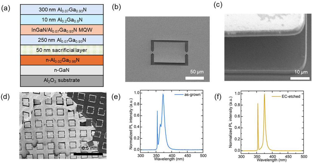
Figure 1: (a) Epitaxial structure of III-nitride device layers with 50nm sacrificial layer before electrochemical etch; (b)–(d) scanning electron microscopy (SEM) images of III-nitride film after etch. PL spectra of structure measured with 355nm laser excitation: (e) before and (f) after etching.
To prepare for the electrochemical etching, trenches were cut into the overlying device layers to expose the sacrificial layer. The trench patterns included two thin tethers to anchor the platelets. The trenches were formed via reactive ion etch.
The electrochemical etch used the sample as the anode with an indium connection to the voltage bias, while the cathode consisted of platinum wire. The electrolyte was 68% nitric acid, which enabled a redox reaction to take place with an applied voltage, cutting into the sacrificial layer. Once the etch process stabilized, the lateral etch speed was around 10–20μm/minute.
The researchers report: “The thickness of the film is approximately 600nm, significantly thinner than typical GaN thin films obtained by laser lift-off.”
The surface roughness of the etched surface from atomic force microscopy (AFM) scans over a 2μmx2μm area was 0.5nm. The team comments: “The roughness is orders of magnitude lower than that of typically reported III-nitride films using the electrochemical etching process with lower silicon doping or using other types of etching.”
The platelets could be transferred to carrier substrates either using polymer stamps or adhesive tape. The tethers broke easily during the transfer step, giving a clean separation of devices from the surrounding material.
The active region of the device material contained two InGaN quantum wells (QW) separated by AlGaN barriers. Photoluminescence (PL) with 355nm laser excitation showed two peaks: a narrow 355nm line from the pump, and a wider 11nm full-width at half maximum (FWHM) peak at ~374nm wavelength from the multiple QWs. In PL spectra from the as-grown samples, there was also a small peak at 364nm attributed to the underlying GaN template. The wider bandgaps of the AlGaN layers were outside the range of the laser excitation.
For the lifted device layers, the MQW peak shifts to 276nm, and narrows to 5.9nm FWHM. The shift and narrowing could be due to strain relaxation in the released device layers, “but still falls within the expected wafer-scale emission non-uniformity,” according to the team. The narrower peak “is likely due to the micro-cavity effect, resulting from the mirror-like, smooth AlGaN surface produced by the electrochemical etching process.”
The researchers comment: “The absence of a GaN-related PL peak indicates the film is completely detached from the substrate, while the strong and preserved MQW emission indicates the InGaN quantum wells are still intact throughout the electrochemical etching process.”
The electrochemical lift-off technique was applied to blue InGaN LED structures transferred to a silicon substrate (Figure 2). The bonding between the silicon and flipped p-GaN contact was through palladium/gold, acting as a p-electrode.
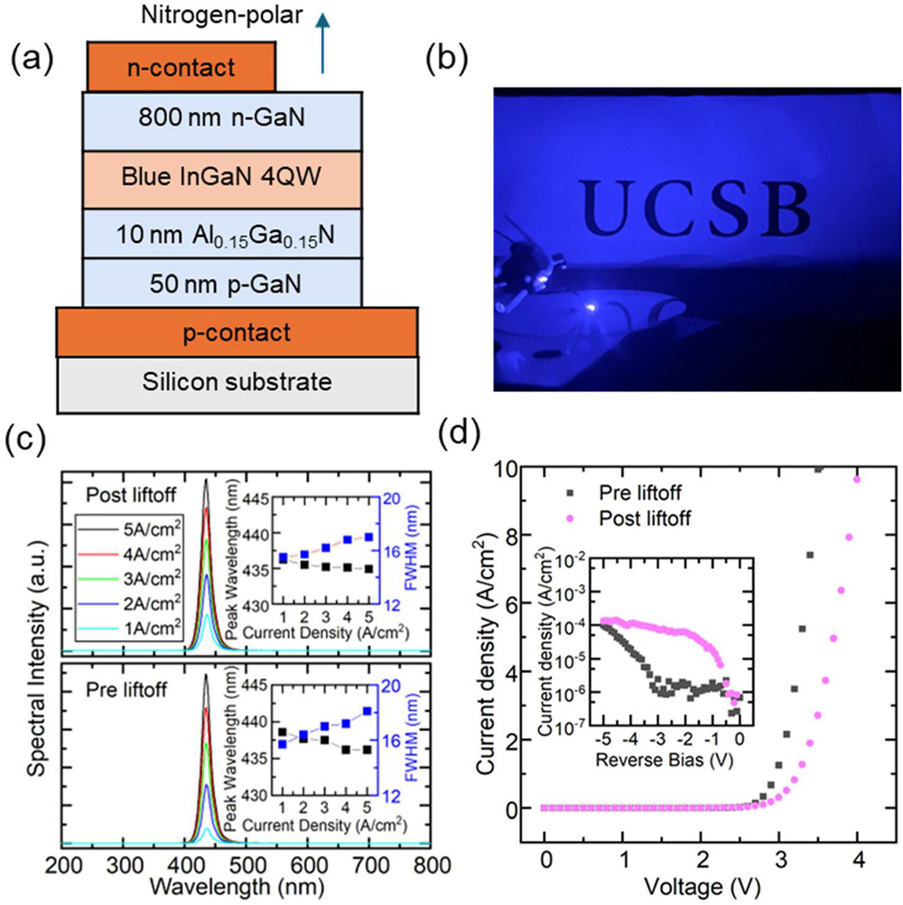
Figure 2: (a) Structure of InGaN-based blue LEDs transferred to silicon. (b) Image of single 100μmx100μm blue LED with 1mA injection current. (c) Electroluminescence (EL) spectra at different current densities before and after lift-off; inset: peak wavelength and FWHM changes. (d) The current density–voltage (J–V) behavior of single blue LED before and after lift-off under forward bias; inset: leakage current under reverse bias before and after lift-off.
The electrical performance of the device after lift-off and transfer showed some degradation with higher series resistance and current leakage under reverse bias. The researchers mainly attribute the higher series resistance to an “unoptimized metal electrode (which is a soldered indium dot) on the bonded surface.” The increased leakage current at lower bias is, they write, “likely due to increased surface leakage from the exposed sidewalls created during the lift-off process.”
The researchers hope that future optimizations of surfaces and interfaces will tackle these issues.
Vertical thin-film micro-light-emitting-diodes LLO InGaN
https://doi.org/10.1063/5.0280302
The author Mike Cooke is a freelance technology journalist who has worked in the semiconductor and advanced technology sectors since 1997.


