


News: Optoelectronics
16 October 2025
Indium arsenide quantum dot laser full MBE on (100) silicon
Researchers based in the UK and France have reported the growth of indium arsenide (InAs) quantum dots (QDs) in gallium arsenide (GaAs) by molecular beam epitaxy (MBE) using a V-grooved silicon (Si) substrate with (100) orientation, as used for mainstream complementary metal-oxide-semiconductor (CMOS) electronics manufacturing [Makhayeni Mtunzi et al, J. Phys. D: Appl. Phys., v58, p405101, 2025]. The team fabricated O-band (1260–1360nm) QD lasers operating up 90°C temperatures.
The team, from University College London, University of Southampton, Swansea University, University of Surrey and the University of Warwick in the UK and University Grenoble Alpes in France, comments: “This work establishes a simplified CMOS-compatible pathway for monolithic integration of III–V QD lasers on silicon, addressing critical challenges in defect suppression. The results serves as a vision for the future of seamlessly integrated electronic–photonic platforms on silicon.”
Such platforms are aimed at high-speed optical communication and computing applications, which require increasing integration of optical and CMOS electronics data/signal processing.
Although MOVPE is advantageous for the growth of buffers on silicon, MBE tends to provide better QD performance. Hybrid approaches combining the two methods would seem logical, but this adds complexity, and “may constrain scalability,” the team believes: “Achieving all MBE-grown InAs/GaAs QD lasers on CMOS-compatible (001) Si is therefore a critical step toward a cost-effective and practical integration pathway.”
The (100) Si orientation is not ideal for III-V growth and usually (111) Si substrates are used. The use of V-grooves enables (111) Si facets to be presented to the III-V growth process: metal-organic vapor phase epitaxy (MOVPE) or molecular beam epitaxy (MBE). The team stresses their use of just MBE: “Unlike previous approaches that combine metal–organic vapor phase epitaxy and MBE processes or employ homoepitaxial silicon regrowth to form (111) facets, our method uses substrates with pre-defined (111) facet exposure, avoiding additional surface engineering.”
The (111) V-groove facets aligned to the [110] direction were created in an 8-inch diameter (100) Si substrate by deep-ultraviolet photolithography, inductively coupled plasma etching, photoresist removal, and a series of hydrofluoric acid and tetramethylammonium hydroxide (TMAH) wet etch treatments. The groove width was 350nm, giving a sawtooth profile.
The V-groove material was diced into 2.1cmx2.1cm squares for the MBE growth.
The QD structure aimed at 1.3μm wavelength emission (Figure 1) was grown based on optimized growth parameters for aluminium arsenide (AlAs) nucleation and a GaAs buffer, dislocation filter layer (DFL) strained-layer superlattice (SLS), and dot-in-well (DWELL) structures.
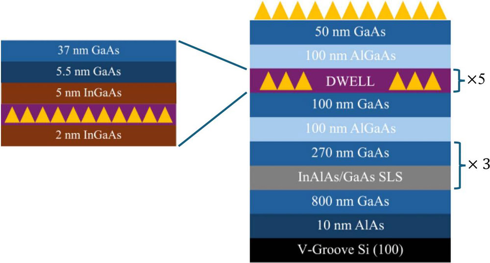
Figure 1: Schematic InAs QD structure featuring three dislocation filter layer (DFL) repeats and five dot-in-well (DWELL) stack. A top uncapped QD layer was used for optimization analysis.
The V-grooves were found to be effective in avoiding anti-phase boundaries (APBs) and in reducing defects. The researchers comment: “The symmetrical geometry of the V-groove promotes effective defect annihilation, as dislocations propagating along opposing Si (111) facets are directed toward the apex of the sawtooth structure. Their convergence at this point increases the likelihood of mutual annihilation, thereby limiting the propagation of defects into the upper epitaxial layers.”
The threading dislocation density (TDD) reached as low as 2.91x10⁷/cm2 at the GaAs buffer surface. An optimized QD structure with 5.88x10¹⁰/cm2 dot density had a 34.6meV full-width at half maximum (FWHM) photoluminescence peak.
For the laser diodes, the team added an extra DFL along with contact and cladding layers: 300nm n-GaAs contact, 1400nm n- and p-type Al0.4Ga0.6As cladding around the DWELL active layers, and 400nm p-GaAs top contact.
This material was fabricated into 25μm-wide broad-area InAs/GaAs QD Fabry–Pérot laser diodes. The p-electrode was sputtered titanium/gold, and the n-type metal stack was evaporated nickel/gold-germanium/nickel/gold. The wafer was annealed and thinned to 180nm before cleaving into 2mm-long laser bars.
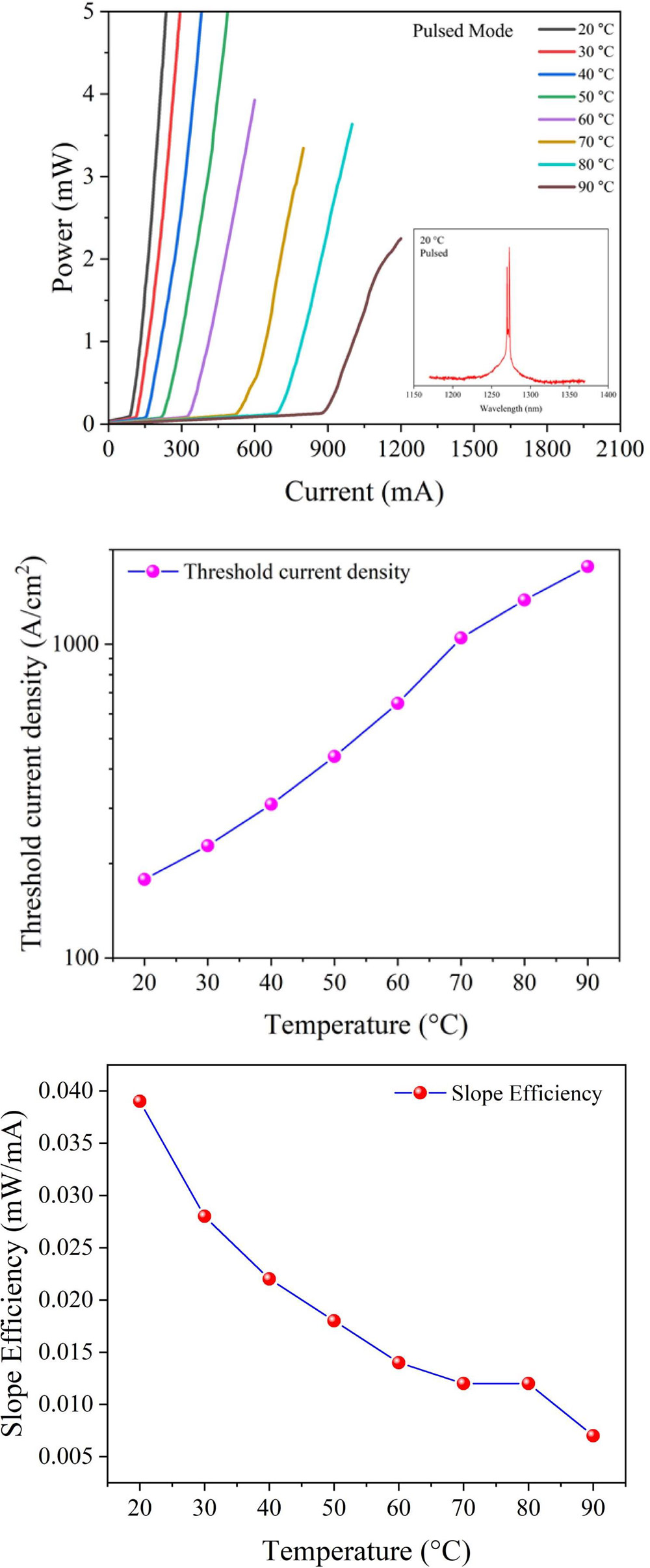
Figure 2: (a) Light–current (L–I) characteristics of QD laser under pulsed-mode injection, measured from 20°C to 90°C. Inset: emission spectra at room temperature (RT). (b) Threshold current density as a function of temperature. (c) Slope efficiency variation.
The room temperature (RT) performance characteristics gave 88.7mA threshold current (177.4A/cm2). The laser continued operating up to 90°C (Figure 2). The temperature variation of the threshold had a T0 characteristic of 28.4K. The variation in slope efficiency, T1, was 48.5K.
https://doi.org/10.1088/1361-6463/ae074b
The author Mike Cooke is a freelance technology journalist who has worked in the semiconductor and advanced technology sectors since 1997.


