


News: Microelectronics
15 October 2025
Navitas supporting 800VDC power architecture for NVIDIA’s next-gen AI factory computing platforms
Navitas Semiconductor Corp of Torrance, CA, USA — which provides GaNFast gallium nitride (GaN) and GeneSiC silicon carbide (SiC) power semiconductors — has announced progress in its development of advanced medium- and high- 800VDC voltage GaN and SiC power devices to enable the 800VDC power architecture announced by NVIDIA of Santa Clara, CA, for next-generation AI factory computing platforms.
Picture: From the grid to the GPU, Navitas’ GaN and SiC technologies power every stage of the AI data center.
With the emergence of the AI factory, a new class of data centers purpose-built for large-scale, synchronous AI and high-performance computing (HPC) workloads has introduced a set of power challenges, notes Navitas. Traditional enterprise and cloud data centers, which rely on legacy 54V in-rack power distribution, are no longer able to meet the multi-megawatt rack densities required by today’s accelerated computing platforms. These challenges call for a fundamental architectural shift, it adds.
800VDC power distribution provides:
- higher efficiency by reducing resistive losses and copper usage;
- scalable infrastructure to deliver MW-scale rack power with highly compact solutions;
- global alignment with the IEC’s low-voltage DC (LVDC) classification (≤1500VDC);
- simplified power distribution with efficient thermal management.
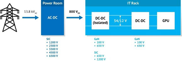
The 800VDC architecture enables direct conversion from 13.8kVAC utility power to 800VDC within the data-center power room or perimeter. By leveraging solid-state transformers (SSTs) and industrial-grade rectifiers, this approach eliminates multiple traditional AC/DC and DC/DC conversion stages, maximizing energy efficiency, reducing losses, and improving overall system reliability.
The 800VDC distribution directly powers IT racks, eliminating the need for additional AC–DC conversion stages, and is stepped down through two high-efficiency DC–DC stages (800VDC to 54V/12VDC, and then to point-of-load GPU voltages), to drive advanced infrastructure such as the NVIDIA Rubin Ultra platform.
These AI factories demand unprecedented levels of power density, efficiency and scalability, which can be enabled by Navitas’ high-performance GaNFast and GeneSiC technologies.
As a pure-play wide-bandgap power semiconductor company, Navitas says that it delivers GaN and SiC technologies that enable high-efficiency and high-power-density power conversion across every stage of the AI data center, from the utility grid to the GPU.
Navitas says that its new 100V GaN FET portfolio delivers superior efficiency, power density and thermal performance in advanced dual-sided cooled packages. These FETs are specifically optimized for the lower-voltage DC–DC stages on GPU power boards, where ultra-high density and thermal management are critical to meet the demands of next-generation AI compute platforms. Samples, datasheets and evaluation boards are available for qualified customers.
Additionally, these high-efficiency 100V GaN FETs are fabricated on a 200mm GaN-on-silicon process through a new strategic partnership with Taiwanese foundry Powerchip Semiconductor Manufacturing Corp (PSMC), enabling scalable, high-volume manufacturing.
Navitas’ 650V GaN portfolio includes a new line of high-power GaN FETs, alongside GaNSafe power ICs, which integrate control, drive, sensing and built-in protection features. This ensures what is claimed to be exceptional robustness and reliability, supporting the demanding performance and safety requirements of next-generation AI infrastructure.
The GaNSafe platform features ultra-fast short-circuit protection (maximum 350ns response), 2kV ESD protection on all pins, elimination of negative gate drive, and programmable slew-rate control. All these features are controlled with 4-pins, allowing the package to be treated like a discrete GaN FET, requiring no VCC pin.
Enabled by over 20 years of SiC innovation, GeneSiC proprietary ‘trench-assisted planar’ provides what is claimed to be exceptional performance over temperature, delivering high-speed, cool-running operation for high-power, high-reliability applications. GeneSiC technology is said to offer the industry’s broadest voltage range, spanning from 650V to 6500V, and has been implemented in multiple megawatt-scale energy storage and grid-tied inverter projects, including collaborations with the US Department of Energy (DoE).
“As NVIDIA drives transformation in AI infrastructure, we’re proud to support this shift with advanced GaN and SiC power solutions that enable the efficiency, scalability and reliability required by next-generation data centers,” says Navitas’ president & CEO Chris Allexandre. “As the industry moves rapidly toward megawatt-scale AI computing platforms, the need for more efficient, scalable and reliable power delivery becomes absolutely critical. The transition from legacy 54V architectures to 800VDC is not just evolutionary, it’s transformational,” he adds. “Navitas is undergoing a fundamental transformation, driven by the convergence of GaN and SiC technologies to power the world’s most advanced systems. From grid to GPU, our focus now extends far beyond mobile, as we address the megawatt-scale demands of AI factories, smart energy infrastructure, and industrial platforms with differentiated, high-performance power solutions.”
Navitas’ cuts losses in Q2 despite revenue still being down year-on-year


