


News: Suppliers
12 November 2025
RPI-led team demonstrates remote epitaxy with 2–7nm epilayer–substrate distance
Led by Rensselaer Polytechnic Institute (RPI) of Troy, NY, USA, a team that also includes researchers at the National High Magnetic Field Laboratory, Florida State University and SUNY Buffalo has deepened the understanding of remote epitaxy, a manufacturing technique that entails growing high-quality semiconducting films on one substrate and then transferring them to a different one (Ru Jia et al, ‘Long-distance remote epitaxy’, Nature, volume 646, p584–591 (2025)).
Remote epitaxy works by placing a thin buffer layer between a substrate and a growing crystal film. The substrate's atomic structure guides the crystal’s growth through the buffer, but the buffer prevents permanent bonding, so the finished crystal layer can be peeled off and moved elsewhere.
Until now, researchers believed that the remote epitaxy technique only worked with buffer layers less than 1nm thick, and that a thicker layer would almost completely overshadow the subtle electrostatic forces from the substrate that guide the growth of the crystal film.
But recently-graduated RPI materials science Ph.D. student Ru Jia and her lab fellows grew crystals through carbon buffer layers up to 7nm thick — a 600% improvement — and found that they still aligned well with the substrate beneath.
“This work shows that remote epitaxy could be mediated by substrate defects such as dislocation,” says RPI materials science and engineering professor Jian Shi Ph.D. (Jia’s Ph.D. advisor, and a senior author on the paper). “Practically, that widens material choices, improves process windows, and aids scalable membrane release and wafer-recycling strategies in real devices.”
Using a zinc oxide/gallium nitride model system in conjunction with Yan Xin’s team at the National High Magnetic Field Laboratory, Jia and her colleagues discovered that structural defects in the substrate may enable long-distance electrostatic interactions that can influence the structure of the crystal layer. RPI materials science professor Yunfeng Shi Ph.D. and his team validated the findings with computations showing that dislocations may mediate long-distance remote epitaxy.
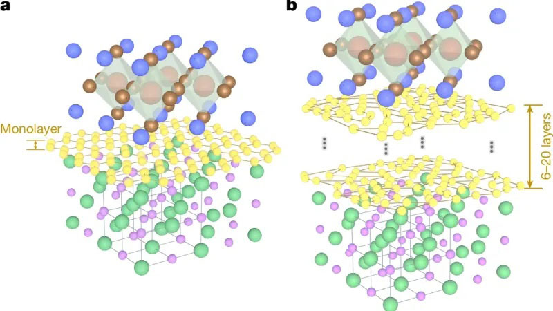
Picture: Schematic diagram of remote epitaxy process. Panel a shows the conventional process with a graphene layer 0.35nm thick, while panel b illustrates the process using a much thicker buffer layer.
“This work would not have been possible without close collaboration among experts in materials growth and characterization, advanced characterization, and atomistic-scale computational simulations,” notes Jian Shi.
The researchers tested their approach with multiple crystal/substrate combinations, demonstrating the universality of their findings. As a proof of concept, they built working photodetectors by transferring perovskite crystal films to flexible substrates, demonstrating the technique's practical viability.
The work suggests that substrate defects, traditionally seen as quality control problems, might be deliberately engineered to control remote epitaxy processes. Manufacturers could, for example, use the technique to program functional ‘islands’ or epilayers in specific locations on their crystal films — a degree of precision that is necessary to fabricate quantum devices that require fine control of crystal growth.
“The paper offers a mechanism — defect-assisted, long-range remote electrostatic interactions — that engineers can intentionally harness to bring about nucleation and alignment in crystal films,” Jian Shi concludes.


