


News: LEDs
20 November 2025
Far-UVC LEDs on c-plane sapphire
The RIKEN Pioneering Research Institute and Saitama University in Japan have reported far-UVC light-emitting diodes fabricated from aluminium gallium nitride (AlGaN) heterostructures directly grown on c-plane sapphire [Taiga Kirihara et al, J. Appl. Phys., v138, p174501, 2025].
Far-UVC radiation is used for microbial disinfection in space and terrestrial environments. The researchers explain: “Humans and animals worldwide die every year from infections caused by multidrug-resistant organisms (MROs) such as methicillin-resistant Staphylococcus aureus (MRSA) and fungi such as Candida auris, as well as Severe Acute Respiratory Syndrome Coronavirus 2 (SARS-CoV-2).”
In human-occupied environments, UVC from existing excimer lamps needs to be specially filtered to wavelengths shorter than 230nm so that the skin or eye’s cornea is not penetrated significantly. These bulky, inefficient lamps also contain toxic gases.
AlGaN-based LEDs with high aluminium content could provide far-UVC radiation, if technical and cost challenges can be met.
The RIKEN/Saitama team believes their work shows the potential of low-cost far-UVC LED devices on c-sapphire, relative to more expensive approaches using bulk AlN wafers or sputtered AlN assisted by double growth and double annealing (DGA). The researchers put the cost of bulk AlN at around $8000 for 2-inch substrates.
The researchers used 1300–1400°C ammonia-pulsed metal-organic chemical vapor deposition (MOCVD) to grow 4μm AlN template layers on c-plane sapphire (Figure 1). The total dislocation density was of order 109/cm2. The surface had fine steps and terraces at the atomic resolution level with root-mean-square 0.068nm surface roughness, according to atomic force microscopy (AFM).
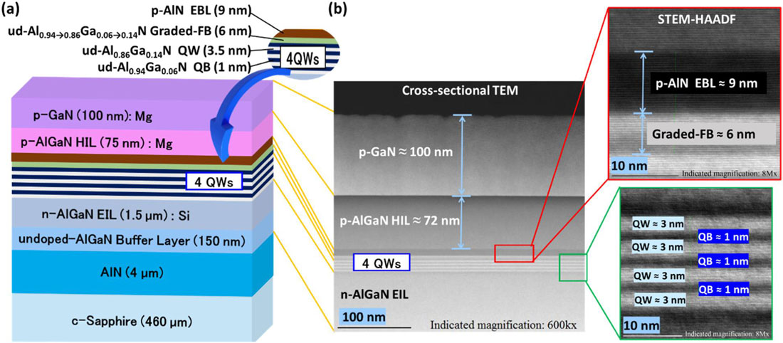
Figure 1: (a) Designed far-UVC LED structure with varying AlN molar fractions in n-AlGaN EIL and (b) structural confirmation of LED with designed parameters.
The far-UVC LED materials consisted of an undoped buffer, an n-type silicon (Si)-doped electron injection layer (EIL), a quantum well (QW) active light-emitting region, an electron-blocking layer (EBL), a p-type magnesium (Mg)-doped hole injection layer (HIL), and a p-GaN contact layer.
The team comments: “The key innovation lies in optimizing the AlN molar fraction (ranging from 0.84 to 0.90) to balance optical transparency and electrical conductivity, critical for achieving efficient 225nm emissions. As the AlN molar fraction increases, the absorption edge of AlGaN shifts to shorter wavelengths, improving the light transmission at 225nm. However, this also raises electrical resistivity due to the reduced carrier concentration, especially beyond the AlN molar fraction of 0.85 using a low Si flow rate.”
The undoped AlGaN buffer was designed to improve crystal quality and to reduce the relaxation ratio of the AlGaN EIL to the 30–35% range. At high AlN fractions, strain affects the nature of the emitted radiation and the transparency of the material route to the outside world, affecting the light extraction efficiency of devices.
One aspect is the positions of the light-hole (LH), heavy-hole (HH) and crystal-field splitting- (CH) hole energies in the valence band structure.
The researchers explain: “When AlxGa1−xN is grown coherently on c-plane AlN, the upper end of the valence band switches from the HH-band to the CH-band at an AlN molar fraction above 0.65 due to lattice distortion and, as a result, the polarization properties change from transverse electric (TE) to transverse magnetic (TM) polarization”
TE-polarized light has better light extraction out of the back-side of the device. The researchers also used thicker QWs and reduced the quantum barrier (QB) thickness to reduce TM emission. Other options for controlling the light polarization and light extraction include using materials with non-polar and semi-polar AlN instead of polar c-plane oriented templates. Such growth methods are almost certainly more challenging, and hence costly.
The researchers found that the optimum Al fraction for the buffer was around 0.88 to balance between efficient current injection and high external quantum efficiency (EQE). A lower 86% Al fraction in the buffer resulted in devices with better current injection for a given voltage, but lower EQE, than for LEDs with 90% Al.
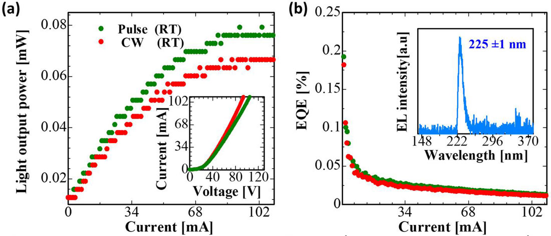
Figure 2: Performance evaluation of 225nm far-UVC LED: (a) current versus light power characteristics (current–voltage inset), (b) current–EQE characteristics (spectral intensity inset).
The resulting LEDs on Al0.88Ga0.12N with a big 400μmx400μm chip size achieved a peak wavelength of 225nm (Figure 2). The peak EQE was around 0.12%, and the maximum light output power (LOP) was 0.08mW.
UVC LEDs AlGaN MOCVD C-plane sapphire
www.riken.jp/en/research/labs/pri
https://doi.org/10.1063/5.0276994
The author Mike Cooke is a freelance technology journalist who has worked in the semiconductor and advanced technology sectors since 1997.


