


News: LEDs
13 November 2025
Inverting Ga-polar LEDs for N-polar benefit
The Institute of High Pressure Physics and the University of Warsaw in Poland have compared the performance of light-emitting diodes (LEDs) composed of opposite polarity III-nitride crystal structures but with the built-in electric field pointing in the more favorable direction usually provided by nitrogen-polar GaN [Tara Brstilo et al, Semicond. Sci. Technol., v40, p105010, 2025].
This was achieved by inverting the LED structure (iLED) with the p-type hole injection layers being grown before the active indium gallium nitride (InGaN) light-emitting region and the n-type electron injector. The Ga-polar iLED achieved around three orders of magnitude (1000x) better light output than the comparison N-polar device.
The researchers comment: “The significantly lower emission intensity obtained for N-polar grown LEDs is most likely associated with the higher incorporation of point defects for growth along this direction.”
Since GaN substrates have electron majority carriers, the team used a tunnel junction to enable hole injection from the buried p-type layers. The team writes: “This work proves that a bottom tunnel junction construction is a reliable way of obtaining LEDs that benefit from an N-polar-like built-in field while using more chemically stable Ga-polar substrate.”
The researchers grew single quantum well (QW) structures for an N-polar LED and Ga-polar iLED by plasma-assisted molecular beam epitaxy (PAMBE) on correspondingly oriented GaN substrates (Figure 1). The use of MBE avoids the presence of hydrogen that tends to passivate p-GaN material.
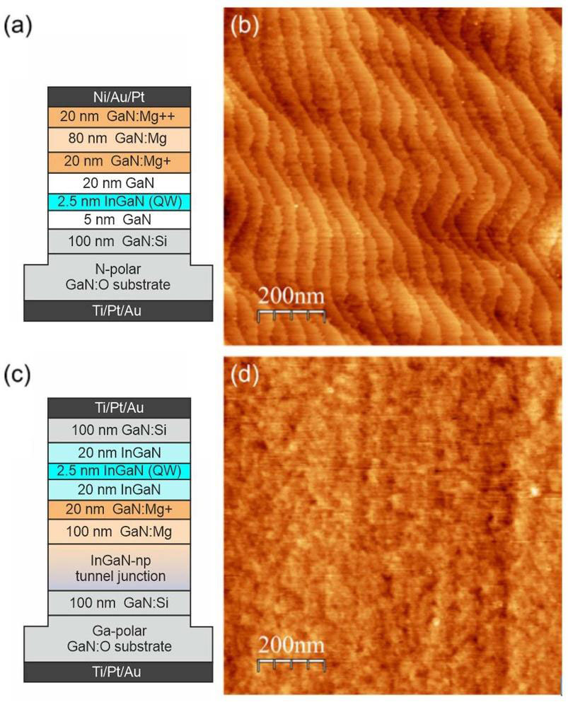
Figure 1: Schematic structures of (a) N-polar LED and (c) Ga-polar iLED. (b,d) Corresponding atomic force microscope (AFM) images obtained before contact deposition.
The presence of hydrogen is unavoidable in the more industrially popular metal-organic chemical vapor deposition process. MOCVD p-type layers need to be activated to remove the hydrogen passivation, typically by high-temperature annealing. This makes it difficult to achieve the iLED structure since the hydrogen would be trapped in the buried layer. This is one of the reasons that p-GaN layers are typically grown last.
The root-mean-square (RMS) roughness of the N- and Ga-polar material surfaces were 0.15nm and 0.3nm, respectively. Post-growth cleaning for the N-polar structure used a cold piranha (sulfuric acid in hydrogen peroxide) solution to avoid hydrochloric acid damage.
For the iLED an InGaN tunnel junction was used to enable vertical current flow between the titanium/platinum/gold metal electrodes suitable for n-type ohmic contact with GaN. The tunnel junction interfaced between the electron and hole majority carrier transport regions to give hole injection into the QW. The n-side of the junction was germanium-doped, while the p-side doping was magnesium.
The InGaN QW was clad by InGaN for the iLED rather than GaN, as for the N-polar LED. “Low-indium-content InGaN barriers were used here instead of GaN to prevent any gallium accumulation during indium-rich growth,” the team explains.
The p-contact electrode for the N-polar LED was nickel/gold/platinum.
The N-polar LED photolithography process used a silicon dioxide protection layer to avoid chemical damage from the photoresist developer solution. This protection was not considered necessary for the iLED. The final devices were 100μm-sided squares.
The Ga-polar iLED had a higher turn-on voltage than the N-polar device (Figure 2). This may be due to the voltage-penalty of the tunnel junction, according to the researchers. However, the N-polar device suffered from a high differential resistance, due to significant current leakage. There was also greater variation in current–voltage performance across different N-polar devices.
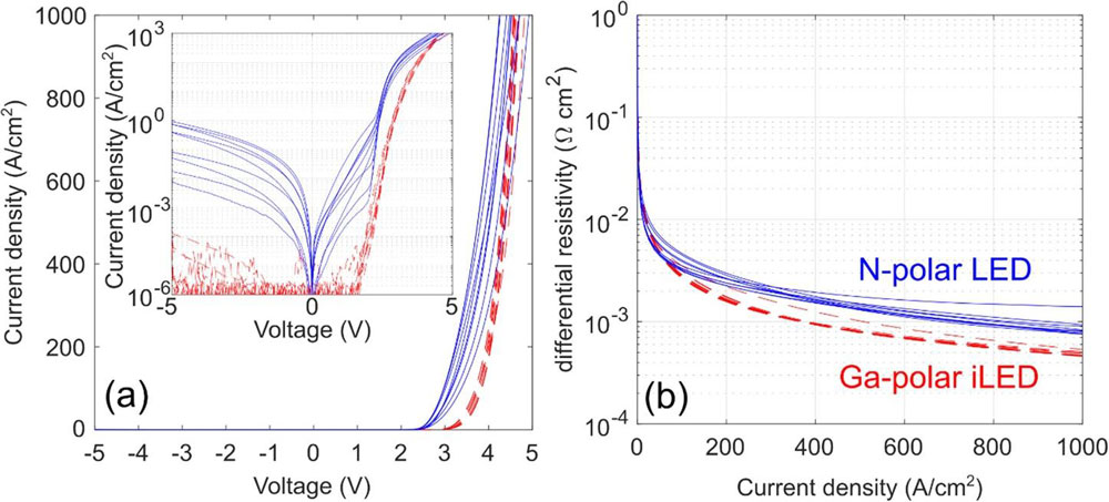
Figure 2: Electrical characterization of representative N-polar (solid blue) and Ga-polar (dashed red) LEDs. (a) Current density versus voltage characteristics, with inset semi-logarithmic scale version. (b) Differential resistance versus current density, derived from data in (a).
The team comments: “This pronounced discrepancy between the characteristics of devices on different parts of the wafer could be indicative of the important role of impurity incorporation, such as background oxygen, which can be non-uniform and can partially passivate p-type conductivity. Additionally, the lower chemical stability of the N-polar surface led to the creation of leakage paths during processing.”
The N-polar devices reached 200A/cm2 current density between 3V and 3.5V bias, while the iLEDs needed 4V. The lower differential resistance of the iLEDs was likely due to lower contact resistance from the n-type GaN with the metal electrodes, compared with p-GaN.

Figure 3: (a) Calculated EQE versus current density for N-polar (left axis) and Ga-polar (right axis) devices and (b) measured optical power variation for same devices.
The Ga-polar iLED achieved much higher estimated external quantum efficiency and measured light output power than the N-polar LED (Figure 3). For the output power, the difference was around three orders of magnitude (1000x).
https://doi.org/10.1088/1361-6641/ae0e45
The author Mike Cooke is a freelance technology journalist who has worked in the semiconductor and advanced technology sectors since 1997.


